SAE 81C90/91
07Feb95@09:05h Intermediate Version
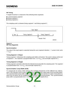
Bit Timing
A regular bit period is composed of the following three segments:
● synchronization segment
● timing segment 1
● timing segment 2.
The sampling point is between timing segment 1 and timing segment 2.
Figure 6
Bit Time Segments
Synchronization
The edge of the input signal is expected during the sync segment (duration = 1 system clock cycle
= 1 tSCL).
Timing Segment 1 (TSeg1)
Timing segment 1 determines the sampling point within a bit period. This point is always at the end
of segment 1. The segment is programmable from 1 to 16 tSCL (see bit-length register BL1).
Timing Segment 2 (TSeg2)
Timing segment 2 provides extra time for internal processing after the sampling point. The segment
is programmable from 1 to 8 tSCL (see bit-length register BL1).
Synchronization Jump Width (SJW)
To compensate for phase shifts between the oscillator frequencies of the different bus stations,
each CAN controller must be able to synchronize to the relevant signal edge of the incoming signal.
The synchronization jump width (SJW) determines the maximum number of system clock pulses by
which the bit period can be lengthened or shortened for resynchronization. The synchronization
jump width is programmable from 1 to 4 tSCL (see bit-length register BL2).
Semiconductor Group
31

 INFINEON [ Infineon ]