SAE 81C90/91
07Feb95@09:05h Intermediate Version
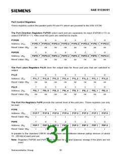
Port Control Registers
These registers control the parallel ports P0 and P1 which are provided in the SAE 81C90.
The Port Direction Registers PxPDR select each port pin separately for input (PxPDR.n=’0’) or
output (PxPDR.n=’1’). After reset the ports are switched as inputs.
P1PDR
7
6
5
4
3
2
1
0
Address: 2C
P1PD.7 P1PD.6 P1PD.5 P1PD.4 P1PD.3 P1PD.2 P1PD.1 P1PD.0
H
Reset Value: 00
rw
rw
rw
rw
rw
rw
rw
rw
H
P0PDR
7
6
5
4
3
2
1
0
Address: 28
P0PD.7 P0PD.6 P0PD.5 P0PD.4 P0PD.3 P0PD.2 P0PD.1 P0PD.0
rw rw rw rw rw rw rw rw
H
Reset Value: 00
H
The Port Latch Registers PxLR store the output data for those port pins that are switched to
output.
P1LR
7
6
5
4
3
2
1
0
Address: 2E
P1L.7
rw
P1L.6
rw
P1L.5
rw
P1L.4
rw
P1L.3
rw
P1L.2
rw
P1L.1
rw
P1L.0
rw
H
Reset Value: 00
H
P0LR
7
6
5
4
3
2
1
0
Address: 2A
P0L.7
rw
P0L.6
rw
P0L.5
rw
P0L.4
rw
P0L.3
rw
P0L.2
rw
P0L.1
rw
P0L.0
rw
H
Reset Value: 00
H
The Port Pin Registers PxPR provide the current level of the port pins. These registers can only
be read.
P1PR
7
P1P.7
r
6
P1P.6
r
5
P1P.5
r
4
P1P.4
r
3
P1P.3
r
2
P1P.2
r
1
P1P.1
r
0
P1P.0
r
Address: 2D
H
Reset Value: 00
H
P0PR
7
P0P.7
r
6
P0P.6
r
5
P0P.5
r
4
P0P.4
r
3
P0P.3
r
2
P0P.2
r
1
P0P.1
r
0
P0P.0
r
Address: 29
H
Reset Value: 00
H
In parallel to the standard CMOS structure there are additional internal pullup devices of about
10...200 kΩ at each port pin.
Note: Registers PxPDR and PxPL may be used for general purpose storage if the ports are not
used.
Semiconductor Group
30

 INFINEON [ Infineon ]