SAE 81C90/91
07Feb95@09:05h Intermediate Version
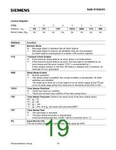
Control Register
CTRL
7
6
5
4
3
2
1
0
Address: 12
RX
rw
TST
rw
TSP
TSOV
rw
SME
rw
TCE
rw
MM
rw
H
Reset Value: 00
rw
rw
H
Bit(field)
MM
Function
Monitor Mode
’0’: Message object 0 operates like all other objects.
’1’: Message object 0 receives all identifiers that are not accepted
by other objects (corresponds to a Basic CAN receive register).
TCE
SME
Transmit Check Enable
’0’: If the transmit check detects an error, there is no intervention.
’1’: If the transmit check detects an error, the message is invalidated by an
error frame and the error counter TCEC is incremented by 1.
If the counter reaches 4, the Bus Off status is initiated and, if enabled, an
interrupt (TCI) is generated.
Sleep Mode Enable
’0’: Normal operation.
’1’: The sleep mode is enabled: the crystal oscillator is deactivated, all other
activities are inhibited.
The wake up is done by a reset signal or by an active signal at the CS pin
or by an input edge going from recessive to dominant at pin Rx0 or Rx1.
TSOV
TSP
Time Stamp Overflow
’0’: There has been no overflow
’1’: There was at least one overflow of the time-stamp timer.
Time Stamp Prescaler (Defines the input clock of the time-stamp timer)
’00’: fBL / 32
’01’: fBL / 64
’10’: fBL / 128
’11’: fBL / 256 (For fBL see baud-rate prescaler BRP).
TST
RX
Time Stamp Test
’0’: The prescaler is activated.
’1’: The time-stamp prescaler is deactivated.
(Only for testing purposes, bit IM = MOD.0 must be set to ’1’).
Input Monitor RX
This bit monitors the actual state of the digital input pin RX0.
Semiconductor Group
18

 INFINEON [ Infineon ]