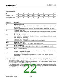
SAE 81C90/91
07Feb95@09:05h Intermediate Version
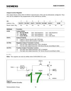
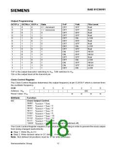
Output Programming
OCTP.n OCTN.n OCP.n Data
TnP
OFF
OFF
OFF
OFF
OFF
OFF
OFF
OFF
OFF
ON
TnN
OFF
OFF
OFF
OFF
ON
OFF
OFF
ON
OFF
OFF
OFF
OFF
ON
OFF
OFF
ON
TXn-Level
float
float
float
float
LOW
float
float
LOW
float
HIGH
HIGH
float
0
0
0
0
0
0
0
0
1
1
1
1
1
1
1
1
0
0
0
0
1
1
1
1
0
0
0
0
1
1
1
1
0
0
1
1
0
0
1
1
0
0
1
1
0
0
1
1
0 = dominant
1 = recessive
0
1
0
1
0
1
0
1
0
1
0
1
0
1
ON
OFF
OFF
ON
ON
OFF
LOW
HIGH
HIGH
LOW
TnP is the output transistor switching to VDD, TnN switches to VSS.
TXn is the output level at the transmit pin.
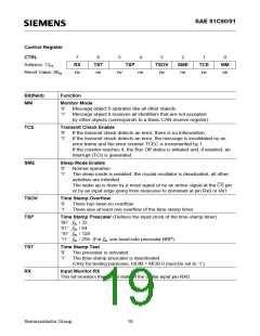
Clock Control Register
The Clock Control Register determines the output frequency at pin CLKOUT which is derived from
the oscillator frequency.
CCR
7
-
6
-
5
-
4
-
3
2
1
0
Address: 14
CC
H
Reset Value: 01
-
-
-
-
w
w
w
w
H
Bit(field)
CC
Function
Clock Output Control
’0000’: f
’0001’: f
’0010’: f
’0011’: f
’0100’: f
’0101’: f
’0110’: f
’0111’: f
’1XXX’: f
= f
= f
= f
= f
= f
= f
= f
= f
CLKOUT
CLKOUT
CLKOUT
CLKOUT
CLKOUT
CLKOUT
CLKOUT
CLKOUT
CLKOUT
OSC
OSC
OSC
OSC
OSC
OSC
OSC
OSC
/ 2
/ 4
/ 6
/ 8
/ 10
/ 12
/ 14
= LOW (clock output is switched off)
The Clock Control Register requires a special protocol for writing in order to prevent the clock output
from being changed inadvertently:
● Step 1: Write 80H to CC
● Step 2: Write desired value to CC (bits 7...4 must be ’0000’)
Note: Not defined bit positions must be ’0’ for write accesses.
Semiconductor Group
17

 INFINEON [ Infineon ]