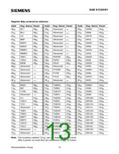
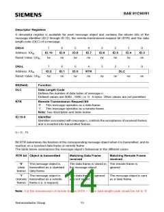
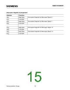
SAE 81C90/91
07Feb95@09:05h Intermediate Version
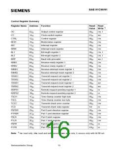
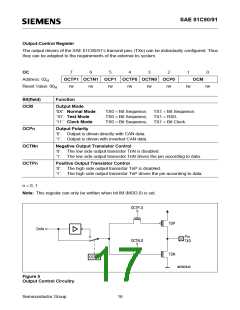
Output-Control Register
The output drivers of the SAE 81C90/91’s transmit pins (TXn) can be individually configured. Thus
they can be adapted to the requirements of the external bs system.
OC
7
6
5
4
3
2
1
0
Address: 02
OCTP1 OCTN1 OCP1 OCTP0 OCTN0 OCP0
rw rw rw rw rw rw
OCM
H
Reset Value: 00
rw
rw
H
Bit(field)
OCM
Function
Output Mode
’0X’: Normal Mode:
’10’: Test Mode:
’11’: Clock Mode:
TX0 = Bit Sequence, TX1 = Bit Sequence.
TX0 = Bit Sequence, TX1 = RX0.
TX0 = Bit Sequence, TX1 = Bit Clock.
OCPn
Output Polarity
’0’: Output is driven directly with CAN data.
’1’: Output is driven with inverted CAN data.
OCTNn
OCTPn
Negative Output Transistor Control
’0’: The low side output transistor TnN is disabled.
’1’: The low side output transistor TnN drives the pin according to data.
Positive Output Transistor Control
’0’: The high side output transistor TnP is disabled.
’1’: The high side output transistor TnP drives the pin according to data.
n = 0, 1
Note: This register can only be written when bit IM (MOD.0) is set.
Figure 5
Output Control Circuitry
Semiconductor Group
16

 INFINEON [ Infineon ]