S29GL01GP
S29GL512P
S29GL256P
S29GL128P
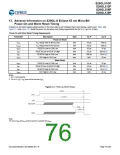
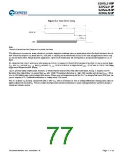
Figure 13.2 Warm Reset Timing
Note:
The sum of tRP and tRH must be equal to or greater than tRPH.
The differences in power-on timing should not present a migration challenge for most applications where the flash interfaces directly
with a Host that requires oscillator and PLL lock prior to initiating the first boot read access to the flash. In applications which may
access the flash within 300 µs of power application, some circuit modification will be required to accommodate migration to GL-S
flash.
To initiate the first read or write cycle after power on, the GL-S requires CE# or OE# to transition from High to Low no sooner than
tVCS after VCC exceeds VCC_min and VIO exceeds VIO_min. CE# or OE# must be High at least tCEH = 20 ns prior to CE# or OE# falling
edge which initiates the first access.
CE# is ignored during Warm Reset; however, to initiate the first read or write cycle after warm reset, the GL-S requires CE# to
transition from High to Low no sooner than tRH after RESET# transitions from Low to High. CE# must be high at least tCEH = 20 ns
prior to CE# falling edge, which initiates first access. These were not requirements for the GL-P so designs that have CE# fixed low
cannot migrate to GL-S without modification to enable active CE# control.
The GL-S allows VIO to ramp concurrently with or after VCC with no restriction on time or voltage differential. During power ramp no
input is allowed to exceed VIO. The GL-S data sheet provides enhanced direction on power management and control to design a
robust and reliable system.
Document Number: 002-00886 Rev. *B
Page 77 of 83

 INFINEON [ Infineon ]