S29GL01GP
S29GL512P
S29GL256P
S29GL128P
Document Title:S29GL01GP, S29GL512P, S29GL256P, S29GL128P
1 Gbit, 512, 256, 128 Mbit, 3 V, Page Flash with 90 nm MirrorBit Process Technology
Document Number: 002-00886
Orig. of
Change
Submission
Date
Rev.
ECN No.
Description of Change
11/20/2008
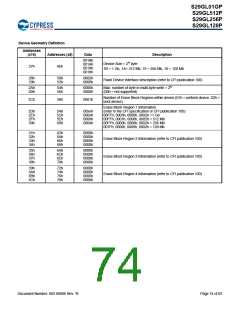
Table S29GL-P Memory Array Command Definitions, x16
Changed number of cycles for Device ID to 6
Changed number of cycles for Write Buffer to 6
Added note regarding the number of cycles in a Write Buffer command
Table S29GL-P Memory Array Command Definitions, x8
Changed number of cycles for Device ID to 6
Changed number of cycles for Write Buffer to 6
Added note regarding the number of cycles in a Write Buffer command
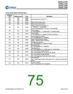
Table System Interface String
Changed value of address 20h (x16) to 0009h and description to
“Typical timeout for buffer write 2n μs”
Added values of 128 Mb-512 Mb densities to address 22h (x16)
Table Device Geometry Definition For address 31h (x16) corrected x8 ad-
dress
11/17/2010
10/22/2012
A13:Performance Characteristics Updated access time options for
S29GL512P
Ordering Information Updated speed options for S29GL512P
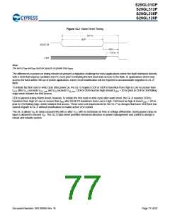
Read Operation Timing Figure Added note
**
-
RYSU
A14:Sector Erase Clarified tSEA
Erase Suspend Clarified tSEA
Writing Commands/Command Sequences
Sub-section RY/BY#: Clarified last sentence
Figure Advanced Sector Protection/Unprotection
Corrected Note numbering
Table S29GL-P Memory Array Command Definitions, x8
Corrected Address for 3rd Cycle of Write-To-Buffer-Abort Reset command
Table System Interface String Changed value of address 20h (x16) to
0006h
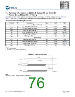
Advance Information on S29GL-R 65 nm MirrorBit Hardware Reset
(RESET#) and Power-up Sequence
Updated section title to Advance Information on S29GL-S Eclipse 65 nm
MirrorBit Power-On and
Warm Reset Timing
Updated section to cover GL-S Power-On and Warm Reset Timing
*A
*B
5051914
RYSU
12/16/2015 Updated to Cypress template
5741254 AESATMP7 05/22/2017 Updated Cypress Logo and Copyright.
Document Number: 002-00886 Rev. *B
Page 82 of 83

 INFINEON [ Infineon ]