S29GL01GP
S29GL512P
S29GL256P
S29GL128P
14. Document History
Document Title:S29GL01GP, S29GL512P, S29GL256P, S29GL128P
1 Gbit, 512, 256, 128 Mbit, 3 V, Page Flash with 90 nm MirrorBit Process Technology
Document Number: 002-00886
Orig. of
Change
Submission
Date
Rev.
ECN No.
Description of Change
10/29/2004 Spansion Publication Number: S29GL-P_00
A0:Initial release
10/20/2005
10/19/2006
A1:Global Revised all sections of document.
A2:Global
Revised all sections of document. Reformatted document to new template.
Changed speed options
for S29GL01GP
11/21/2006 A3:AC Characteristics Erase and Program Operations table: Changed tBUSY to
a maximum specification.
12/18/2006
A4:Global
Changed tACC, tCE specifications on 128 Mb, 256 Mb, and 512 Mb devices.
Added 90 and 100 ns
speed options.
Write Buffer Programming, Sector Erase
Write Buffer Programming Operation, Sector Erase Operation figures:
Deleted “Wait 4 ms” box from
flowcharts.
Password Protection Method Lock Register Program Algorithm figure:
Deleted “Wait 4 ms” box from flowchart.
**
-
RYSU
Read-only Operations table Modified tRC, tACC, tCE, tOE specifications.
Program and Erase Operations tables Changed tDS specification, deleted
write cycle time note.
TSOP Pin and BGA Capacitance table Changed all specifications in table.
05/18/2007
A5:Global
Changed data sheet status to Preliminary.
Deleted references to requirement for external WP# pull-up.
Performance Characteristics Max. Read Access Times table: Added note.
Hardware Reset Deleted note from section.
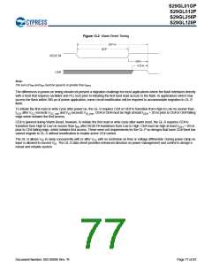
AC Characteristics Reset Timings figure: Deleted note.
Command Definitions tables
S29GL-P Sector Protection Command Definitions tables: Changed “Global
Non-Volatile Freeze” to “Global Volatile Freeze”.
DC Characteristics CMOS Compatible table: Changed ICC1 maximum
current for 5 MHz and MHz test conditions.
Page Read Timings figure Corrected address range for top waveform
Document Number: 002-00886 Rev. *B
Page 79 of 83

 INFINEON [ Infineon ]