S29GL01GP
S29GL512P
S29GL256P
S29GL128P
Document Title:S29GL01GP, S29GL512P, S29GL256P, S29GL128P
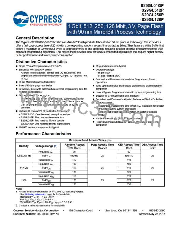
1 Gbit, 512, 256, 128 Mbit, 3 V, Page Flash with 90 nm MirrorBit Process Technology
Document Number: 002-00886
Orig. of
Change
Submission
Date
Rev.
ECN No.
Description of Change
11/20/2009
A12:Table Input/Output Descriptions Removed RFU description
Figure 64-ball Fortified Ball Grid Array Changed all RFU pins to NC pins
Figure 56-pin Standard TSOP (Top View)
Changed all RFU pins to NC pins
Table Autoselect Exit Changed cycle description to Auto Select Exit Command
Table Chip Erase Changed address of last C source code command from
0x000h to 0x555h
Erase Suspend/Erase Resume
Changed first paragraph, second sentence to sector address is “don't care”
for Erase Suspend
Changed sixth paragraph, second sentence to sector address is “don't care”
for Erase Suspend
Tables
Program Suspend
**
-
RYSU
Program Resume
Unlock Bypass Entry
Unlock Bypass Program
Unlock Bypass Reset
Added Byte Address to tables
Unlock Bypass
Third paragraph, first sentence added unlock bypass Sector Erase and
unlock bypass Chip Erase
as valid commands
Changed paragraph, third sentence to sector address of exit command is
“don't care”.
Writing Commands/Command Sequence
Changed tables listed in fourth sentence to Table 6.1-6.4
WP#/ACC Method Changed table listed in Note section to 11.2.
Secured Silicon Sector Entry/Exit Command Sequence
Added source code for program under Table 10.3
Table Secured Silicon Sector Exit Changed Byte and Word addresses of
Exit Cycle to “XXXh”
Figure Test Setup Changed test setup to show only a load of CL
Table Test Specification Removed Output Load Test Condition
Table S29GL-P Erase and Program Operations
Removed tGHWL
Table S29GL-P Alternate CE# Controlled Erase and Program
Operations
Changed description of tGHEL to (OE# High to CE# Low)
Change Note 2 to “DC Characteristics
TSOP Pin and BGA Package Capacitance
Changed RESET# values.
Document Number: 002-00886 Rev. *B
Page 81 of 83

 INFINEON [ Infineon ]