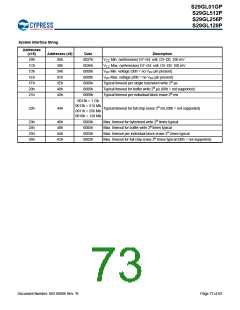
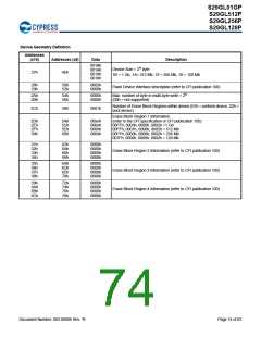
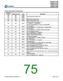
S29GL01GP
S29GL512P
S29GL256P
S29GL128P
13. Advance Information on S29GL-S Eclipse 65 nm MirrorBit
Power-On and Warm Reset Timing
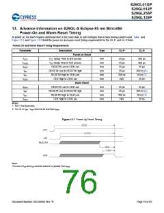
At power on, the flash requires additional time in the reset state to self configure than it does during a warm reset. Table and
Figure 13.1 and Figure 13.2 detail the power on and warm reset timing requirements for the GL-P, and GL-S flash.
Power On and Warm Reset Timing Requirements
Parameter
Description
Type
GL-P
GL-S
Power on Reset
tVCS
tVIOS
tRPH
tRP
VCC Setup Time to first access
VIO Setup Time to first access
RESET# Low to CE# Low
RESET# Low to RESET# High
RESET# High to CE# Low
CE# High to CE# Low
min
min
min
min
min
min
35 µs
35 µs
35 µs
35 µs
200 ns
N/A
300 µs
300 µs
35 µs
200 ns (2)
50 ns (2)
20 ns
tRH
tCEH
Warm Reset
tRPH
tRP
RESET# Low to CE# Low
RESET# Low to RESET# High
RESET# High to CE# Low
CE# High to CE# Low
min
min
min
min
35 µs
35 µs
200 ns
N/A
35 µs
200 ns (2)
50 ns (2)
20 ns
tRH
tCEH
Notes:
1. N/A = Not Applicable.
2. For GL-S, tRP + tRH must not be less than tRPH.
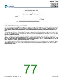
Figure 13.1 Power-Up Reset Timing
Note:
The sum of tRP and tRH must be equal to or greater than tRPH.
Document Number: 002-00886 Rev. *B
Page 76 of 83

 INFINEON [ Infineon ]