IMW120R020M1H
™
CoolSiC 1200 V SiC Trench MOSFET
1 Package
1
Package
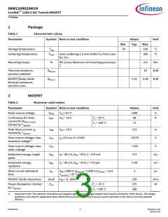
Table 1
Characteristic values
Symbol Note or test condition
Parameter
Values
Typ.
Unit
Min.
Max.
150
Storage temperature
Soldering temperature
Tstg
-55
°C
°C
Tsold
wave soldering 1.6 mm (0.063 in.) from case
for 10 s
260
Mounting torque
M
M3 screw, Maximum of mounting processes:
3
0.6
62
Nm
K/W
K/W
Thermal resistance,
junction-ambient
Rth(j-a)
Rth(j-c)
MOSFET/body diode
thermal resistance,
junction-case
0.31
0.40
2
MOSFET
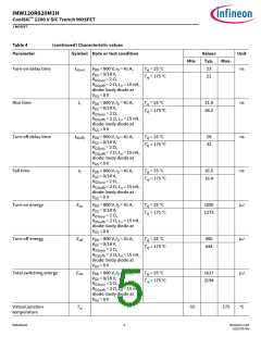
Table 2
Maximum rated values
Symbol Note or test condition
Parameter
Values
1200
98
Unit
Drain-source voltage
VDSS
IDDC
Tvj ≥ 25 °C
VGS = 18 V
V
A
Continuous DC drain
current for Rth(j-c,max)
limited by Tvj(max)
Tc = 25 °C
,
Tc = 100 °C
71
Peak drain current, tp
limited by Tvj(max)
IDM
VGS
VGS
EAS
EAR
tSC
VGS = 18 V
213
-10/23
-7/20
721
A
V
Gate-source voltage, max.
transient voltage1)
tp ≤ 0.5 µs, D < 0.001
Gate-source voltage, max.
static voltage
V
Avalanche energy, single
pulse
ID = 40.1 A, VDD = 50 V, L = 0.9 mH
ID = 40.1 A, VDD = 50 V, L = 4.5 µH
mJ
mJ
µs
Avalanche energy,
repetitive
3.58
3
Short-circuit withstand
time
VDD ≤ 800 V, VDS,peak < 1200 V, VGS(on) = 15 V,
Tvj(start) = 25 °C
MOSFET dv/dt robustness
dv/dt
Ptot
VDS = 0...800 V
Tc = 25 °C
150
375
188
V/ns
W
Power dissipation, limited
by Tvj(max)
Tc = 100 °C
1)
Important note: The selection of positive and negative gate-source voltages impacts the long-term behavior of the device. The design
guidelines described in Application Note AN2018-09 must be considered to ensure sound operation of the device over the planned
lifetime.
Datasheet
3
Revision 1.30
2023-05-08

 INFINEON [ Infineon ]