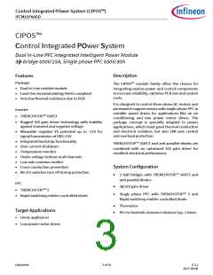
Control Integrated POwer System (CIPOS™)
IFCM15P60GD
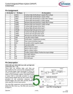
It is recommended for proper work of this product
not to provide input pulse-width lower than 1.5us.
The under-voltage circuit enables the device to
operate at power on when a supply voltage of at
least a typical voltage of VDDUV+ = 12.1V is present.
The IC shuts down all the gate drivers’ power
outputs, when the VDD supply voltage is below
VDDUV- = 10.4V. This prevents the external power
switches from critically low gate voltage levels
during on-state and therefore from excessive power
dissipation.
The integrated gate drive provides additionally a
shoot through prevention capability which avoids
the simultaneous on-state of two gate drivers of the
same leg (i.e. HO1 and LO1, HO2 and LO2, HO3 and
LO3). When two inputs of a same leg are activated,
only former activated one is activated so that the
leg is kept steadily in a safe state.
A minimum deadtime insertion of typically 380ns is
also provided by driver IC, in order to reduce cross-
conduction of the external power switches.
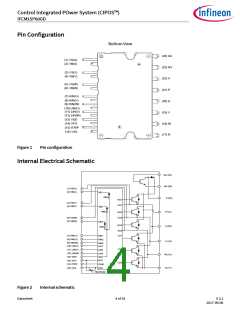
VB(U,V,W) and VS(U,V,W) (High side supplies, Pin 1 -
6)
VB to VS is the high side supply voltage. The high
side circuit can float with respect to VSS following
the external high side power device emitter voltage.
Due to the low power consumption, the floating
driver stage is supplied by integrated bootstrap
circuit.
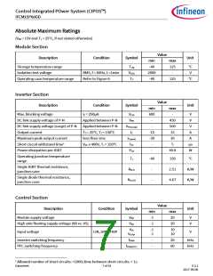
VFO (Fault-output and NTC, Pin 14)
The VFO pin indicates a module failure in case of
under voltage at pin VDD or in case of triggered
over current detection at ITRIP. A pull-up resistor is
externally required to bias the NTC.
The under-voltage detection operates with a rising
supply threshold of typical VBSUV+ = 12.1V and a
falling threshold of VBSUV- = 10.4V.
CIPOS
VDD
VFO
RON,FLT
From ITRIP - Latch
VS(U,V,W) provide
a high robustness against
1
negative voltage in respect of VSS of -50V
transiently. This ensures very stable designs even
under rough conditions.
VSS
From UV detection
Thermistor
Figure 5
Internal circuit at pin VFO
N (Low side emitter, Pin 17)
The same pin provides direct access to the NTC,
which is referenced to VSS. An external pull-up
resistor connected to +5V ensures that the resulting
voltage can be directly connected to the
microcontroller.
The low side emitters are available for current
measurements. It is recommended to keep the
connection to pin VSS as short as possible in order
to avoid unnecessary inductive voltage drops.
W, V, U (High side emitter and low side collector,
Pin 18 - 20)
ITRIP (Over current detection function, Pin 15)
CIPOS™ provides an over current detection
These pins are motor U, V, W input pins
function by connecting the ITRIP input with the
motor current feedback. The ITRIP comparator
threshold (typ. 0.47V) is referenced to VSS ground.
An input noise filter (typ: tITRIPMIN = 530ns) prevents
the driver to detect false over-current events.
Over current detection generates a shut down of all
outputs of the gate driver after the shutdown
propagation delay of typically 1000ns.
P (Positive bus input voltage, Pin 21)
The high side IGBTs and PFC diode cathode are
connected to the bus voltage. It is noted that the
bus voltage does not exceed 450V.
X, NX, GX (Single boost PFC, Pins 22-24)
These pins are emitter, collector and gate of IGBT
for single boost PFC.
VDD, VSS (Low side control supply and reference,
Pin 13, 16)
VDD is the low side supply and it provides power
both to input logic and to low side output power
stage. Input logic is referenced to VSS ground.
Datasheet
6 of 18
V 2.2
2017-09-06

 INFINEON [ Infineon ]