Control Integrated POwer System (CIPOS™)
IFCM15P60GD
Table of contents
Table of contents...................................................................................................................................................2
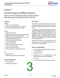
CIPOS™ Control Integrated POwer System............................................................................................................3
Features
..................................................................................................................................................................3
Target Applications......................................................................................................................................................3
Description ..................................................................................................................................................................3
System Configuration..................................................................................................................................................3
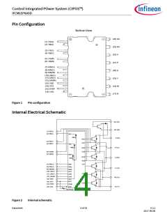
Pin Configuration...................................................................................................................................................4
Internal Electrical Schematic.................................................................................................................................4
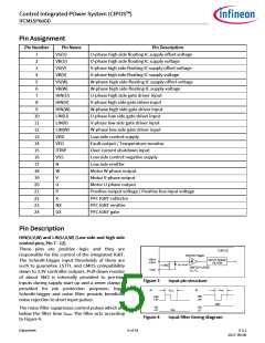
Pin Assignment ......................................................................................................................................................5
Pin Description ......................................................................................................................................................5
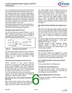
HIN(U,V,W) and LIN(U,V,W) (Low side and high side control pins, Pin 7 - 12)............................................................5
VFO (Fault-output and NTC, Pin 14) ............................................................................................................................6
ITRIP (Over current detection function, Pin 15)..........................................................................................................6
VDD, VSS (Low side control supply and reference, Pin 13, 16)...................................................................................6
VB(U,V,W) and VS(U,V,W) (High side supplies, Pin 1 - 6) .............................................................................................6
N (Low side emitter, Pin 17).........................................................................................................................................6
W, V, U (High side emitter and low side collector, Pin 18 - 20) ...................................................................................6
P (Positive bus input voltage, Pin 21)..........................................................................................................................6
X, NX, GX (Single boost PFC, Pins 22-24) .....................................................................................................................6
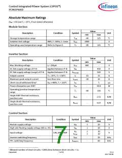
Absolute Maximum Ratings ...................................................................................................................................7
Module Section ............................................................................................................................................................7
Inverter Section............................................................................................................................................................7
Control Section ............................................................................................................................................................7
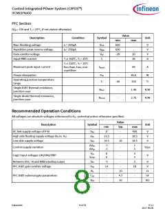
PFC Section ..................................................................................................................................................................8
Recommended Operation Conditions ...................................................................................................................8
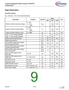
Static Parameters ..................................................................................................................................................9
Inverter Section............................................................................................................................................................9
PFC Section ................................................................................................................................................................10
Bootstrap Parameters .........................................................................................................................................10
Dynamic Parameters ...........................................................................................................................................11
Inverter Section..........................................................................................................................................................11
PFC Section ................................................................................................................................................................12
Thermistor...........................................................................................................................................................13
Mechanical Characteristics and Ratings ..............................................................................................................13
Circuit of a Typical Application ............................................................................................................................14
Switching Times Definition ..................................................................................................................................15
Package Outline...................................................................................................................................................16
Revision history ...................................................................................................................................................17
Datasheet
2 of 18
V 2.2
2017-09-06

 INFINEON [ Infineon ]