Control Integrated POwer System (CIPOS™)
IFCM15P60GD
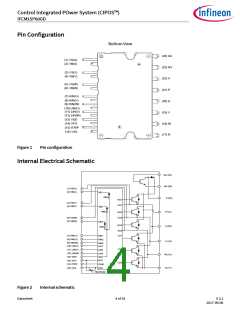
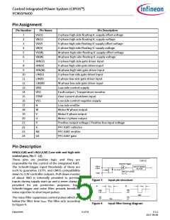
Pin Assignment
Pin Number
Pin Name
Pin Description
U-phase high side floating IC supply offset voltage
U-phase high side floating IC supply voltage
V-phase high side floating IC supply offset voltage
V-phase high side floating IC supply voltage
W-phase high side floating IC supply offset voltage
W-phase high side floating IC supply voltage
U-phase high side gate driver input
V-phase high side gate driver input
W-phase high side gate driver input
U-phase low side gate driver input
V-phase low side gate driver input
W-phase low side gate driver input
Low side control supply
1
VS(U)
2
VB(U)
VS(V)
VB(V)
VS(W)
VB(W)
HIN(U)
HIN(V)
HIN(W)
LIN(U)
LIN(V)
LIN(W)
VDD
VFO
ITRIP
VSS
3
4
5
6
7
8
9
10
11
12
13
14
15
16
17
18
19
20
21
22
23
24
Fault output / Temperature monitor
Over current shutdown input
Low side control negative supply
Low side emitter
N
W
Motor W-phase output
V
Motor V-phase output
U
Motor U-phase output
P
Positive output voltage / Positive bus input voltage
PFC IGBT collector
X
NX
PFC IGBT emitter
GX
PFC IGBT gate
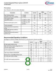
Pin Description
HIN(U,V,W) and LIN(U,V,W) (Low side and high side
control pins, Pin 7 - 12)
These pins are positive logic and they are
responsible for the control of the integrated IGBT.
The Schmitt-trigger input thresholds of them are
such to guarantee LSTTL and CMOS compatibility
down to 3.3V controller outputs. Pull-down resistor
of about 5k is internally provided to pre-bias
inputs during supply start-up and a zener clamp is
provided for pin protection purposes. Input
Schmitt-trigger and noise filter provide beneficial
noise rejection to short input pulses.
CIPOS
Schmitt-Trigger
HINx
LINx
INPUT NOISE
FILTER
UZ=10.5V
5k
SWITCH LEVEL
VIH; VIL
VSS
Figure 3
Input pin structure
a)
b)
tFILIN
tFILIN
HIN
LIN
HIN
LIN
high
HO
LO
HO
LO
The noise filter suppresses control pulses which are
below the filter time tFILIN. The filter acts according
to Figure 4.
low
Figure 4
Input filter timing diagram
Datasheet
5 of 18
V 2.2
2017-09-06

 INFINEON [ Infineon ]