Quasi-Resonant, 800V CoolSET™ in DS0-12 Package
Functional Description
To avoid mis-triggering caused by the voltage spike across the shunt resistor at the turn on of the main power
switch, a leading edge blanking time, tLEB, is applied to the output of the comparator. In other words, once the
gate drive is turned on, the minimum on time of the gate drive is the leading edge blanking time.
In addition, there is a maximum on time, tOnMax, limitation implemented in the IC. Once the gate drive has been
in high state longer than the maximum on time, it will be turned off to prevent the switching frequency from
going too low because of long on time.
3.4
Current Limitation
There is a cycle by cycle current limitation realized by the current limit comparator to provide an over-current
detection. The source current of the MOSFET is sensed via a sense resistor RCS. By means of RCS the source
current is transformed to a sense voltage VCS which is fed into the pin CS. If the voltage VCS exceeds an internal
voltage limit, adjusted according to the Mains voltage, the comparator immediately turns off the gate drive.
To prevent the Current Limitation process from distortions caused by leading edge spikes, a Leading Edge
Blanking time (tLEB) is integrated in the current sensing path.
A further comparator is implemented to detect dangerous current levels (VCSSW) which could occur if one or
more transformer windings are shorted or if the secondary diode is shorted. To avoid an accidental latch off, a
spike blanking time of tCSSW is integrated in the output path of the comparator.
3.4.1
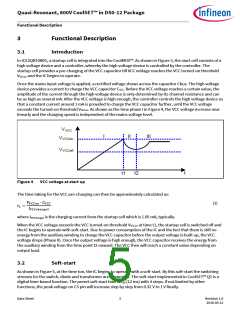
Foldback Point Correction
When the main bus voltage increases, the switch on time becomes shorter and therefore the operating
frequency is also increased. As a result, for a constant primary current limit, the maximum possible output
power is increased which is beyond the converter design limit.
To avoid such a situation, the internal foldback point correction circuit varies the VCS voltage limit according to
the bus voltage. This means the VCS will be decreased when the bus voltage increases. To keep a constant
maximum input power of the converter, the required maximum VCS versus various input bus voltage can be
calculated, which is shown in Figure 7.
Figure 7
Variation of the VCS limit voltage according to the IZC current
According to the typical application circuit, when MOSFET is turned on, a negative voltage proportional to bus
voltage will be coupled to auxiliary winding. Inside CoolSET™ Q1, an internal circuit will clamp the voltage on
ZC pin to nearly 0 V. As a result, the current flowing out from ZC pin can be calculated as
Data Sheet
9
Revision 1.0
2016-05-12

 INFINEON [ Infineon ]