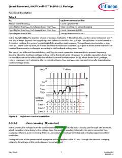
Quasi-Resonant, 800V CoolSET™ in DS0-12 Package
Functional Description
resulted if the voltage across the shunt resistor at CS pin hits the threshold VcsB (0.34 V). A turn-off can also be
triggered if the duty ratio exceeds the maximal duty ratio DmaxB (50%). In operation, the output flip-flop will be
reset by one of these signals which come first.
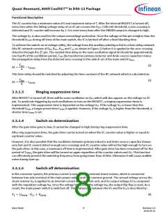
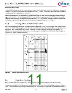
If the output load is still low, the feedback signal decreases as the PWM section is operating. When feedback
signal reaches the low threshold VFBBOff (3.0 V), the internal bias is reset again and the PWM section is disabled
until next time regulation signal increases beyond the VFBBOn (3.6 V) threshold. If working in Active Burst Mode
the feedback signal is changing like a saw tooth between VFBBOff and VFBBOn shown in Figure 9.
3.5.3
Leaving Active Burst Mode Operation
The feedback voltage immediately increases if there is a high load jump. This is observed by a comparator. As
the current limit is 34% during Active Burst Mode a certain load is needed so that feedback voltage can exceed
VFBLB (4.5 V). After leaving active burst mode, maximum current can now be provided to stabilize VOUT. In
addition, the up/down counter will be set to 1 immediately after leaving Active Burst Mode. This is helpful to
decrease the output voltage undershoot.
VFB
Leaving
Active Burst
Mode
Entering
Active Burst
Mode
VFBLB
VFBBOn
VFBBOff
VFBEB
Time to 7th zero and
Blanking Window (tBEB
t
)
VCS
Current limit level during
Active Burst Mode
1.0V
VCSB
VVCC
t
t
t
VVCCoff
VO
Max. Ripple < 1%
Figure 9
Signals in Active Burst Mode
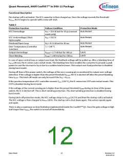
3.6
Protection Functions
The IC provides full protection functions. The following table summarizes these protection functions.
During operation, the VCC voltage is continuously monitored. In case of an under-voltage or an over-voltage,
the IC is reset and the main power switch is then kept off. After the VCC voltage falls below the threshold VVCCoff
,
Data Sheet
11
Revision 1.0
2016-05-12

 INFINEON [ Infineon ]