Quasi-Resonant, 800V CoolSET™ in DS0-12 Package
Functional Description
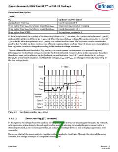
The ZC counter has a minimum value of 0 and maximum value of 7. After the internal MOSFET is turned off,
every time when the falling voltage ramp of on ZC pin crosses the VZCCT (100 mV) threshold, a zero crossing is
detected and ZC counter will increase by 1. It is reset every time after the DRIVER output is changed to high.
The voltage VZC is also used for the output overvoltage protection. Once the voltage at this pin is higher than the
threshold VZCOVP during off-time of the main switch, the IC is latched off after a fixed blanking time.
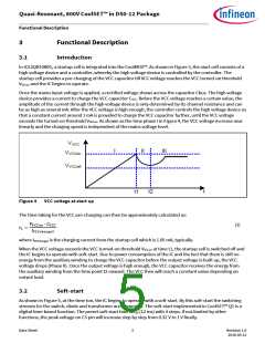
To achieve the switch-on at voltage valley, the voltage from the auxiliary winding is fed to a time delay network
(the RC network consists of DZC, RZC1, R ZC2 and C ZC as shown in Figure 1) before it is applied to the zero-crossing
detector through the ZC pin. The needed time delay to the main oscillation signal Δt should be approximately
one fourth of the oscillation period, TOSC (by transformer primary inductor and drain-source capacitor) minus
the propagation delay from the detected zero-crossing to the switch-on of the main switch tdelay
.
푇
(2)
표푠푐
∆푡 =
− 푡푑푒푙푎푦
4
This time delay should be matched by adjusting the time constant of the RC network which is calculated as:
푇
(3)
표푠푐
∆푡 =
− 푡푑푒푙푎푦
4
3.3.1.3
Ringing suppression time
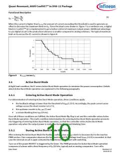
After MOSFET is turned off, there will be some oscillation on VDS, which will also appear on the voltage on ZC
pin. To avoid mis-triggering by such oscillations to turn on the MOSFET, a ringing suppression timer is
implemented. This suppression time is depended on the voltage VZC. If the voltage VZC is lower than the
threshold VZCRS, a longer preset time tZCRS2 is applied. However, if the voltage VZC is higher than the threshold, a
shorter time tZCRS1 is set.
3.3.1.4
Switch on determination
After the gate drive goes to low, it cannot be changed to high during ring suppression time.
After ring suppression time, the gate drive can be turned on when the ZC counter value is higher or equal to
up/down counter value.
However, it is also possible that the oscillation between primary inductor and drain-source capacitor damps
very fast and IC cannot detect enough zero crossings and ZC counter value will not be high enough to turn on
the gate drive. In this case, a maximum off time is implemented. After gate drive has been remained off for the
period of TOffMax, the gate drive will be turned on again regardless of the counter values and VZC. This function
can effectively prevent the switching frequency from going lower than 20 kHz. Otherwise it will cause audible
noise during start up.
3.3.1.5
Switch off determination
In the converter system, the primary current is sensed by an external shunt resistor, which is connected
between low-side terminal of the main power switch and the common ground. The sensed voltage across the
shunt resistor VCS is applied to an internal current measurement unit, and its output voltage V1 is compared
with the regulation voltage VFB. Once the voltage V1 exceeds the voltage VFB, the output flip-flop is reset. As a
result, the main power switch is switched off. The relationship between the V1 and the VCS is described by:
(4)
푉 = 퐺푃푊푀 ∙ 푉 + 푉
1
퐶푆
푃푊푀
Data Sheet
8
Revision 1.0
2016-05-12

 INFINEON [ Infineon ]