CCM-PFC
ICE2PCS06/G
Functional Description
voltage at pin VCOMP. This block has been designed
to support the wide input voltage range (85-265VAC).
Vout
D1
L1
From
Full-wave
Retifier
R3
3.7
PWM Logic
C2
R7
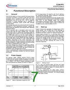
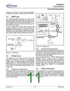
The PWM logic block prioritizes the control input
signals and generates the final logic signal to turn on
the driver stage. The speed of the logic gates in this
R4
block, together with the width of the reset pulse TOFFMIN
are designed to meet a maximum duty cycle DMAX of
95% at the GATE output.
,
Gate Driver
Current Loop
+
PWM Generation
In case of high input currents which result in Peak
Current Limitation, the GATE will be turned off
immediately and maintained in off state for the current
PWM cycle. The signal Toffmin resets (highest priority,
overriding other input signals) both the current limit
latch and the PWM on latch as illustrated in Figure 13.
VIN
GATE
Nonlinear
Gain
OTA1
3V
Av(IIN
)
VSENSE
t
VCOMP
Current
Limit Latch
ICE2PCS06/G
Q
Peak Current
Limit
G1
S
R
HIGH =
turn GATE on
L1
R6
PWM on
Latch
C4
C5
Current Loop
PWM on signal
S
L2
R
Q
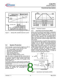
Figure 14 Voltage Loop
3.8.2 Enhanced Dynamic Response
Toffmin
385ns
Due to the low frequency bandwidth of the voltage loop,
the dynamic response is slow and in the range of about
several 10ms. This may cause additional stress to the
bus capacitor and the switching transistor of the PFC in
the event of heavy load changes.
Figure 13 PWM Logic
3.8
Voltage Loop
The IC provides therefore a “window detector” for the
feedback voltage VVSENSE at pin
6 (VSENSE).
The voltage loop is the outer loop of the cascaded
control scheme which controls the PFC output bus
voltage VOUT. This loop is closed by the feedback
sensing voltage at VSENSE which is a resistive divider
tapping from VOUT. The pin VSENSE is the input of
OTA1 which has an accurate internal reference of 3V
(±2%). Figure 14 shows the important blocks of this
voltage loop.
Whenever VVSENSE exceeds the reference value (3V)
by +5%, it will act on the nonlinear gain block which in
turn affect the gate drive duty cycle directly. This
change in duty cycle is bypassing the slow changing
VCOMP voltage, thus results in a fast dynamic
response of VOUT
.
3.9
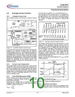
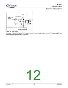
Output Gate Driver
3.8.1
Voltage Loop Compensation
The compensation of the voltage loop is installed at the
VCOMP pin (see Figure 14). This is the output of OTA1
and the compensation must be connected at this pin to
ground. The compensation is also responsible for the
soft start function which controls an increasing AC input
current during start-up.
The output gate driver is a fast totem pole gate drive. It
has an in-built cross conduction currents protection and
a Zener diode Z1 (see Figure 15) to protect the external
transistor switch against undesirable over voltages.
The maximum voltage at pin 8 (GATE) is typically
clamped at 15V.
Version 1.1
11
Mar 2010

 INFINEON [ Infineon ]