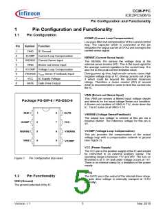
CCM-PFC
ICE2PCS06/G
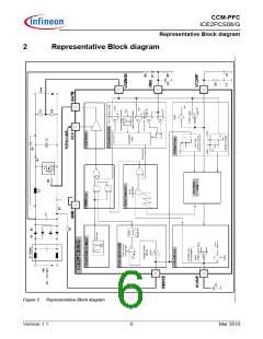
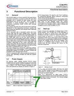
Functional Description
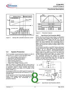
3.4.2
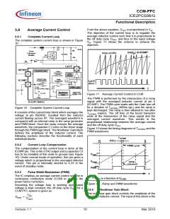
Soft Over Current Control (SOC)
The IC is designed not to support any output power
that corresponds to a voltage lower than -0.75V at the
ISENSE pin. A further increase in the inductor current,
which results in a lower ISENSE voltage, will activate
the Soft Over Current Control (SOC). This is a soft
control as it does not directly switch off the gate drive.
It acts on the nonlinear gain block to result in a reduced
PWM duty cycle.
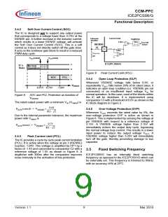
Current Limit
1.5V
Full-wave
Rectifier
Deglitcher
300ns
Turn Off
Driver
C2
ISENSE
R2
1.43x
IINDUCTOR
R1
OP1
POUT(rated)
POUT(max)
ICE2PCS06/G
IC’s
Normal
State Operation
Figure 9
3.4.4
Peak Current Limit (PCL)
SOC
PCL
Open Loop Protection (OLP)
Whenever VSENSE voltage falls below 0.6V, or
equivalently VOUT falls below 20% of its rated value, it
indicates an open loop condition (i.e. VSENSE pin not
connected) or an insufficient input voltage VIN for
normal operation. In this case, most of the blocks within
the IC will be shutdown. It is implemented using
comparator C3 with a threshold of 0.6V as shown in the
IC block diagram in Figure 2.
VISENSE
-0.61V -0.75V
-1.04V
0
Figure 8
SOC and PCL Protection as function of
VISENSE
The rated output power with a minimum VIN (VINMIN) is
0.61
POUT(rated) = VINMIN
´
------------------
3.4.5
Over-Voltage Protection (OVP)
R1 ×
2
Whenever VOUT exceeds the rated value by 5%, the
over-voltage protection OVP is active as shown in
Figure 6. This is implemented by sensing the voltage at
pin VSENSE with respect to a reference voltage of
3.15V. A VSENSE voltage higher than 3.15V will
immediately reduce the output duty cycle, bypassing
the normal voltage loop control. This results in a lower
input power to reduce the output voltage VOUT. A
VSENSE voltage higher than 3.25V will immediately
turn off the gate, thereby preventing damage to bus
capacitor.
Due to the internal parameter tolerance, the maximum
power with VINMIN is
0.75
POUT(max) = VINMIN
´
------------------
R1 ×
2
3.4.3
Peak Current Limit (PCL)
The IC provides a cycle by cycle peak current limitation
(PCL). It is active when the voltage at pin 3 (ISENSE)
reaches -1.04V. This voltage is amplified by OP1 by a
factor of -1.43 and connected to comparator C2 with a
reference voltage of 1.5V as shown in Figure 9. A
deglitcher with 300ns after the comparator improves
noise immunity to the activation of this protection.
3.5
Fixed Switching Frequency
ICE2PCS06/G has an internally fixed switching
frequency as opposed to the ICE2PCS01/G which can
be externally set. This frequency is trimmed to 65kHz
with an accuracy ±5% at 25oC.
Version 1.1
9
Mar 2010

 INFINEON [ Infineon ]