CCM-PFC
ICE2PCS06/G
Functional Description
From the above equation, DOFF is proportional to VIN.
The objective of the current loop is to regulate the
average inductor current such that it is proportional to
the off duty cycle DOFF, and thus to the input voltage
VIN. Figure 11 shows the scheme to achieve the
objective.
3.6
Average Current Control
3.6.1
Complete Current Loop
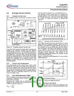
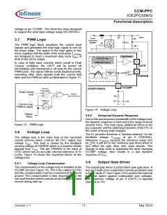
The complete system current loop is shown in Figure
10.
Vout
L1
D1
R3
R4
From
Full-wave
Retifier
ave(IIN) at ICOMP
ramp profile
C2
R7
R2
R1
GATE
ISENSE
Current Loop
voltage
proportional to
averaged
Inductor current
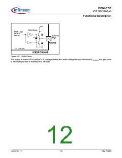
Gate
Driver
Current Loop
Compensation
PWM
Comparator
ICOMP
GATE
drive
Q
R
S
C1
OTA2
1.0mS
+/-50uA (linear range)
PWM Logic
t
C3
S2
Input From
Voltage Loop
Nonlinear
Gain
4.2V
Figure 11 Average Current Control in CCM
Fault
The PWM is performed by the intersection of a ramp
signal with the averaged inductor current at pin 5
(ICOMP). The PWM cycle starts with the Gate turn off
for a duration of TOFFMIN (400ns typ.) and the ramp is
kept discharged. The ramp is then allowed to rise after
TOFFMIN expires. The off time of the boost transistor
ends at the intersection of the ramp signal and the
averaged current waveform. This results in the
proportional relationship between the average current
ICE2PCS06/G
Figure 10 Complete System Current Loop
It consists of the current loop block which averages the
voltage at pin ISENSE, resulted from the inductor
current flowing across R1. The averaged waveform is
compared with an internal ramp in the ramp generator
and PWM block. Once the ramp crosses the average
waveform, the comparator C1 turns on the driver stage
through the PWM logic block. The Nonlinear Gain block
defines the amplitude of the inductor current. The
following sections describe the functionality of each
individual blocks.
and the off duty cycle DOFF
.
Figure 12 shows the timing diagrams of TOFFMIN and the
PWM waveforms.
TOFFMIN
400ns
3.6.2
Current Loop Compensation
PWM cycle
The compensation of the current loop is done at the
ICOMP pin. This is the OTA2 output and a capacitor C3
has to be installed at this node to ground (see Figure
10). Under normal mode of operation, this pin gives a
voltage which is proportional to the averaged inductor
current. This pin is internally shorted to 4.2V in the
event of standby mode.
(1)
VCREF
VRAMP
PWM
ramp
released
3.6.3
Pulse Width Modulation (PWM)
t
The IC employs an average current control scheme in
continuous conduction mode (CCM) to achieve the
power factor correction.
Assuming the voltage loop is working and output
voltage is kept constant, the off duty cycle DOFF for a
CCM PFC system is given as
(1)
V
is a function of VICOMP
CREF
Figure 12 Ramp and PWM waveforms
3.6.4 Nonlinear Gain Block
The nonlinear gain block controls the amplitude of the
regulated inductor current. The input of this block is the
VIN
DOFF = -------------
VOUT
Version 1.1
10
Mar 2010

 INFINEON [ Infineon ]