CCM-PFC
ICE2PCS06/G
Functional Description
3
Functional Description
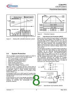
If VCC drops below 11V, the IC is off. The IC will then
be consuming typically 300mA, whereas consuming
10mA during normal operation.
The IC can be turned off and forced into standby mode
by pulling down the voltage at pin 6 (VSENSE) to lower
than 0.6V. In this standby mode, the current
consumption is reduced to 300mA. Other condition that
can result in the standby mode is when a Brown-out
condition occurs, ie pin 4 (VINS) <0.71V.
3.1
General
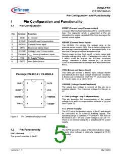
The ICE2PCS06/G is a 8 pin control IC for power factor
correction converters. It comes in both DIP and DSO
packages and is suitable for wide range line input
applications from 85 to 265 VAC. The IC supports
converters in boost topology and it operates in
continuous conduction mode (CCM) with average
current control.
It is a design derivative from the ICE2PCS01/G with the
differences in the supporting functions, namely the
input brown-out detection and internal fixed switching
frequency 65kHz.
3.3
Start-up
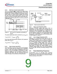
Figure 4 shows the operation of voltage loop’s OTA1
during startup. The VCOMP pin is pull internally to
ground via switch S1 during UVLO and other fault
conditions (see later section on “System Protection”).
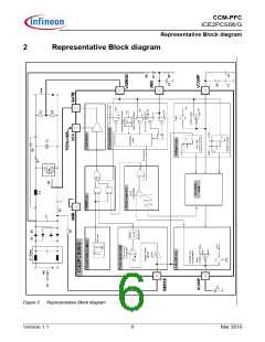
The IC operates with a cascaded control; the inner
current loop and the outer voltage loop. The inner
current loop of the IC controls the sinusoidal profile for
the average input current. It uses the dependency of
the PWM duty cycle on the line input voltage to
determine the corresponding input current. This means
the average input current follows the input voltage as
long as the device operates in CCM. Under light load
condition, depending on the choke inductance, the
system may enter into discontinuous conduction mode
(DCM) resulting in a higher harmonics but still meeting
the Class D requirement of IEC 1000-3-2.
During power up when VOUT is less than 83% of the
rated level, OTA1 sources an output current, maximum
30mA into the compensation network at pin 5 (VCOMP)
causing the voltage at this pin to rise linearly. This
results in a controlled linear increase of the input
current from 0A thus reducing the stress on the
external component.
The outer voltage loop controls the output bus voltage.
Depending on the load condition, OTA1 establishes an
appropriate voltage at VCOMP pin which controls the
amplitude of the average input current.
VSENSE
R4
x VOUT
)
(
R3 + R4
The IC is equipped with various protection features to
ensure safe operating condition for both the system
and device.
OTA1
3V
VCOMP
3.2
Power Supply
protect
S1
R6
C4
An internal under voltage lockout (UVLO) block
monitors the VCC power supply. As soon as it exceeds
11.8V and both voltages at pin 6 (VSENSE) >0.6V and
pin 4 (VINS) >1.5V, the IC begins operating its gate
drive and performs its Startup as shown in Figure 3.
C5
ICE2PCS06/G
Figure 4
Startup Circuit
.
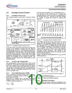
As VOUT has not reached within 5% from the rated
value, VCOMP voltage is level-shifted by the window
detect block as shown in Figure 5, to ensure there is
fast boost up output voltage.
(VVSENSE > 0.6 V) (VVSENSE < 0.6 V)
(VVSENSE > 0.6 V)
AND (VVINS > 1.5 V) OR (VVINS < 0.8 V) AND (VVINS > 1.5 V)
VCC
When VOUT approaches its rated value, OTA1’s
sourcing current drops and so does the level shift of the
window detect block is removed. The normal voltage
loop then takes control.
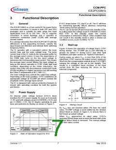
11.8 V
11.0 V
OFF
t
IC's
State
Start
Up
Normal
Operation
Normal
Operation
Open loop/
Standby
OFF
Figure 3
State of Operation respect to VCC
Version 1.1
7
Mar 2010

 INFINEON [ Infineon ]