EZ-PD™ CCG7D Automotive USB Type-C and Buck-boost Controller
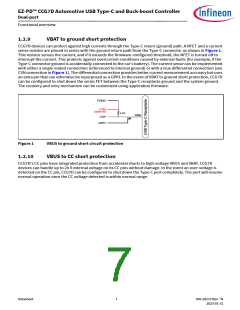
Dual-port
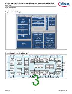
Functional overview
1.2.2
VCONN switches
CCG7D’s internal LDO voltage regulator is capable of powering a 100 mW VCONN supply for electronically marked
cable assemblies (EMCA), VCONN-powered devices (VPD), and VCONN-powered accessories (VPA) as defined in
the USB Type-C specification. All circuitry including VCONN switches and OCP is integrated in the device. In the
event the VCONN current exceeds the VCONN OCP limit, CCG7D can be configured to shut down the Type-C port
after a certain number of user configurable retries. The port can be re-enabled after a physical disconnect.
1.2.3
VBUS UVP and OVP
VBUS undervoltage and overvoltage faults are monitored using internal resistor dividers. The fault thresholds
and response times are user configurable. Refer to the EZ-PD Configuration Utility for more details. In the event
of a UVP or OVP, CCG7D can be configured to shut down the Type-C port after a certain number of user
configurable retries. The port can be re-enabled after a physical disconnect.
1.2.4
VBUS OCP and SCP
VBUS overcurrent and short-circuit faults are monitored using internal current sense amplifiers. Similar to OVP
and UVP, the OCP and SCP fault thresholds and response times are configurable as well. Refer to the EZ-PD
Configuration Utility for more details. In the event of OCP or SCP, CCG7D can be configured to shut down the
Type-C port after a certain number of user configurable retries. The port can be re-enabled after a physical
disconnect.
1.2.5
High-side CSA for VBUS
CCG7D device family supports VBUS current measurement and control using an external resistor (5 mΩ) in series
with the VBUS path. The voltage drop across this resistor is used to measure the average output current. The
same resistor is also used to sense and precisely control the output current in the PPS current foldback mode of
operation.
1.2.6
VBUS discharge control
The chip supports high-voltage (21.5 V) VBUS discharge circuitry. Upon the detection of device disconnection,
faults, or hard resets, the chip will discharge the output VBUS terminals to vSafe5V and/or vSafe0V within the time
limits specified in the USB-PD Specification.
1.2.7
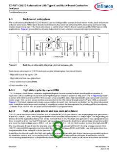
Gate driver for VBUS provider NFET
CCG7D devices have an integrated high-voltage gate driver to drive the gate of an external high-side NFET on the
VBUS provider path. The gate driver drives the load switch that controls the connection between VBUS_IN and
VBUS_C. VBUS_CTRL is the output of this gate driver. To turn off the external NFET, the gate driver drives VBUS_IN
low to 0 V. To turn on the external NFET, it drives the gate to VBUS_IN + 8 V. There is an optional slow turn-on
feature which reduces the high-current spikes on the output. For a typical gate capacitance of 3 nF, a slow turn-on
time of 2 ms to 10 ms is configurable using firmware.
1.2.8
Legacy charge detection and support
CG7D implements battery charger emulation and detection (source and sink) for USB BC.1.2, legacy Apple
charging, Qualcomm Quick Charge 2.0/3.0, and Samsung AFC protocols.
Datasheet
6
002-28172 Rev. *N
2023-01-31

 INFINEON [ Infineon ]