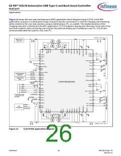
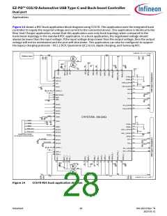
EZ-PD™ CCG7D Automotive USB Type-C and Buck-boost Controller
Dual-port
Applications
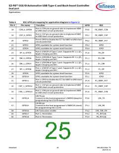
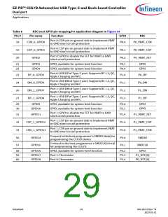
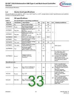
Table 6
Pin #
RSC buck GPIO pin mapping for application diagram in Figure 14
Pin name
Function
GPIO
RSC
Port 0: CSN pin on ground side to implement VBAT
to GND short circuit protection
18
19
20
CSN_0_GPIO0
P0.0
P0_VBAT_CSN
Port 0: CSP pin on ground side to implement VBAT
to GND short circuit protection
CSP_0_GPIO1
GPIO2
P0.1
P0.2
P0_VBAT_CSP
P0_VBAT_FET
Port 0: GPIO to disable the FET for VBAT to GND
short circuit protection
21
22
GPIO3
GPIO4
GPIO, available for system level function
GPIO, available for system level function
P0.3
P0.4
GPIO
GPIO
Port 0: USB DP of Type-C port. Supports BC 1.2, QC,
Apple Charging and AFC
23
24
26
27
DP_0_GPIO5
DM_0_GPIO6
DM_1_GPIO7
DP_1_GPIO8
P1.0
P1.1
P1.2
P1.3
P0_DP
P0_DM
P1_DM
P1_DP
Port 0: USB DM of Type-C port. Supports BC 1.2, QC,
Apple Charging and AFC
Port 1: USB DM of Type-C port. Supports BC 1.2, QC,
Apple Charging and AFC
Port 1: USB DP of Type-C port. Supports BC 1.2, QC,
Apple Charging and AFC
29
30
GPIO9
GPIO, available for system level function
GPIO, available for system level function
P2.0
P2.1
GPIO
GPIO
GPIO10
Port 1: GPIO to disable the FET for VBAT to GND
short circuit protection
31
32
GPIO11
P1.4
P1.5
P1_VBAT_FET
P1_VBAT_CSP
Port 1: CSP pin on ground side to implement VBAT
to GND short circuit protection
CSP_1_GPIO12
Port 1: CSN pin on ground side to implement VBAT
to GND short circuit protection
33
56
57
CSN_1_GPIO13
GPIO14
P1.6
P3.0
P3.1
P1_VBAT_CSN
SWDIO
Connect to the host programmer’s SWDIO (data) for
programming the CCG7D device
Connect to the host programmer’s SWDCLK (clock)
for programming the CCG7D
GPIO15
SWDCLK
58
59
60
GPIO16
GPIO17
GPIO18
GPIO, available for system-level function
Port 1: Thermistor
Port 0: Thermistor
P3.2
P3.3
P3.4
GPIO
P1_NTC[0]
P0_NTC[0]
Datasheet
29
002-28172 Rev. *N
2023-01-31

 INFINEON [ Infineon ]