EZ-PD™ CCG7D Automotive USB Type-C and Buck-boost Controller
Dual-port
Applications
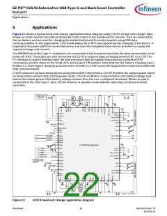
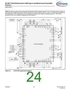
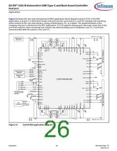
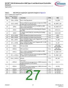
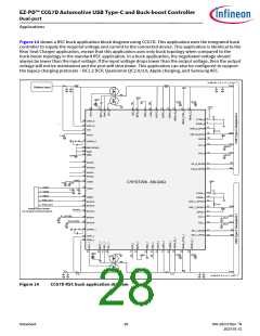
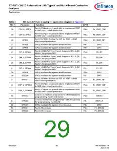
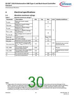
Figure 13 shows the rear seat entertainment (RSE) application block diagram using CCG7D. In the RSE
application, one port is a dedicated charge-only port and the second port is used for charging and streaming
video content to the rear-seat monitor, using a mobile phone, PC, or a tablet. The implementation of the
charging-only port is identical to the RSC application. CCG7D supports display port alternate mode sink in the
port that supports video streaming and controls the external display port multiplexer over I2C. CCG7D also
communicates with the system’s SoC over I2C.
(USB PD, 3.3-21V, 5A)
5 m
5 m
VIN
VBUS
Battery Input
(9V-18V)
VDDD
VDDD
0.1μF
0.1μF
68
67
1
2
5
9
7
8
6
11
12 13
17
14
1μF
4
3
PVDD_0
PGND_0
66
CSNI_0
65
61
62
CSPI_0
VIN
5 m
19
20
GND
CC1
CSP_0_GPIO1
GPIO2
VCCD
0.1μF
10
COMP_0
15
16
CC1_0
CC2_0
390pF
69
64
34
GND (EPAD)
GND
GND
CC2
390pF
AGND
HPI_INT
33
CSN_1_GPIO13
Host Processor/
Billboard
DP
HPI_SDA
HPI_SCL
29
30
23
24
DP_0_GPIO5
DM_0_GPIO6
GPIO9
GPIO10
DM
I2CM_SCL
I2CM_SDA
21
22
GPIO3
GPIO4
Display Port
Mux
HPD
18
CSN_0_GPIO0
63
25
VDDD
10μF
VDDD
VDDD
CYPD7299-68LDXS
0.1μF
1μF
48
49
VDDD
1
2
3
PVDD_1
PGND_1
0.1μF 1μF
AGND
XRES
28
57
56
XRES
5 m
LIN_RX
LIN_TX
SWD_CLK
4
5
32
31
GND
GPIO15
GPIO14
CSP_1_GPIO12
GPIO11
SWD_DAT
LIN_TXR_EN
58
Programming Header
– not needed for final
production
GPIO16
CC1
CC2
37
36
P1_NTC[0]
P0_NTC[0]
59
60
CC1_1
CC2_1
GPIO17
GPIO18
390pF
390pF
42
COMP_1
27
26
DP
DP_1_GPIO8
DM_1_GPIO7
LIN_RX
DM
55
54
CSPI_1
CSNI_1
LIN
LIN_TX
Transceiver
LIN_TXR_EN
52
39
35
38
53 51 50
47 43
45 44 46
41 40
VDDD
VDDD
0.1μF
0.1μF
VBUS
VIN
5 m
5 m
(USB PD, 3.3-21V, 5A)
Figure 13
CCG7D RSE application diagram
Datasheet
26
002-28172 Rev. *N
2023-01-31

 INFINEON [ Infineon ]