IDT72T7285/72T7295/72T72105/72T72115 2.5V TeraSync
16,384 x 72, 32,768 x 72, 65,536 x 72, 131,072 x 72
72-BIT FIFO
COMMERCIAL AND INDUSTRIAL
TEMPERATURE RANGES
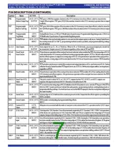
PINDESCRIPTION(CONTINUED)
Symbol
Name
I/OTYPE
Description
(2)
TRST
JTAGReset
HSTL-LVTTL TRSTisanasynchronousresetpinfortheJTAGcontroller.TheJTAGTAPcontrollerdoesnotautomatically
INPUT
resetuponpower-up,thusitmustberesetbyeitherthissignalorbysettingTMS=HIGHforfiveTCKcycles.
IftheTAPcontrollerisnotproperlyresetthentheFIFOoutputswillalwaysbeinhigh-impedance.IftheJTAG
functionisusedbuttheuserdoesnotwanttouseTRST,thenTRSTcanbetiedwithMRStoensureproper
FIFOoperation.IftheJTAGfunctionis notusedthenthis signalneeds tobetiedtoGND.
WEN
WriteEnable
HSTL-LVTTL WhenSynchronousoperationofthewriteporthasbeenselected,WENenablesWCLKforwritingdatainto
INPUT
theFIFOmemoryandoffsetregisters.IfAsynchronousoperationofthewriteporthasbeenselected,the
WENinputshouldbetiedLOW.
WCS
WriteChipSelect HSTL-LVTTL This pindisables the write portdata inputs whenthe device write portis configuredforHSTLmode. This
INPUT provides added power savings.
WCLK/ WriteClock/
HSTL-LVTTL IfSynchronousoperationofthewriteporthasbeenselected,whenenabledbyWEN,therisingedgeofWCLK
WR
WriteStrobe
INPUT
writesdataintotheFIFO.IfAsynchronousoperationofthewriteporthasbeenselected,WRwritesdatainto
the FIFO on a rising edge in an Asynchronous manner, (WEN should be tied to its active state).
(1)
WHSTL WritePortHSTL
Select
LVTTL
INPUT
ThispinisusedtoselectHSTLor2.5VLVTTLinputsfortheFIFO.IfHSTLinputsarerequired,thisinputmust
betiedHIGH.OtherwiseitshouldbetiedLOW.
VCC
GND
Vref
+2.5v Supply
GroundPin
I
I
I
These are Vccsupplyinputs andmustbe connectedtothe 2.5Vsupplyrail.
These are Ground pins and must be connected to the GND rail.
Reference
Voltage
ThisisaVoltageReferenceinputandmustbeconnectedtoavoltageleveldeterminedfromthetable,
“RecommendedDCOperatingConditions”.This provides thereferencevoltagewhenusingHSTLclass
inputs.IfHSTLclass inputs arenotbeingused,this pinshouldbetiedLOW.
VDDQ
O/PRailVoltage
I
This pin should be tied to the desired voltage rail for providing power to the output drivers.
NOTES:
1. Inputs should not change state after Master Reset.
2. These pins are for the JTAG port. Please refer to pages 29-31 and Figures 6-8.
8

 IDT [ INTEGRATED DEVICE TECHNOLOGY ]