IDT72T7285/72T7295/72T72105/72T72115 2.5V TeraSync
16,384 x 72, 32,768 x 72, 65,536 x 72, 131,072 x 72
72-BIT FIFO
COMMERCIAL AND INDUSTRIAL
TEMPERATURE RANGES
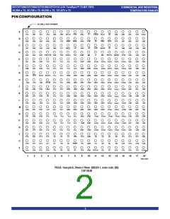
PINDESCRIPTION
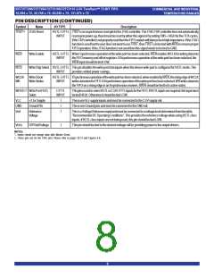
Symbol
Name
I/OTYPE
Description
(1)
ASYR Asynchronous
ReadPort
LVTTL
INPUT
AHIGHonthisinputduringMasterResetwillselectSynchronousreadoperationfortheoutputport.ALOW
willselectAsynchronousoperation.IfAsynchronousisselectedtheFIFOmustoperateinIDTStandardmode.
(1)
ASYW Asynchronous
LVTTL
INPUT
AHIGHonthisinputduringMasterResetwillselectSynchronouswriteoperationfortheinputport.ALOW
willselectAsynchronousoperation.
WritePort
(1)
BE
Big-Endian/
Little-Endian
LVTTL
INPUT
DuringMasterReset, a LOWonBE willselectBig-Endianoperation. AHIGHonBE duringMasterReset
willselectLittle-Endianformat.
(1)
BM
Bus-Matching
LVTTL
INPUT
BM works with IW and OW to select the bus sizes for both write and read ports. See Table 1 for bus size
configuration.
D0–D71 DataInputs
HSTL-LVTTL Datainputsfora72-,36-or18-bitbus.Whenin36-or18-bitmode,theunusedinputpinsareinadon’tcare
INPUT state.
EF/OR EmptyFlag/
HSTL-LVTTL IntheIDTStandardmode,theEFfunctionisselected.EFindicateswhetherornottheFIFOmemoryisempty.
OutputReady
OUTPUT
InFWFTmode,theOR functionis selected.ORindicates whetherornotthereis validdataavailableatthe
outputs.
ERCLK RCLK Echo
HSTL-LVTTL ReadclockEchooutput, onlyavailable whenthe Readis setupforSynchronous mode.
OUTPUT
EREN Read Enable Echo HSTL-LVTTL Read Enable Echo output, only available when the Read is setup for Synchronous mode.
OUTPUT
FF/IR Full Flag/
HSTL-LVTTL Inthe IDTStandardmode, the FF functionis selected. FF indicates whetherornotthe FIFOmemoryis
Input Ready
OUTPUT
full. Inthe FWFTmode, the IR functionis selected. IR indicates whetherornotthere is space available for
writingtotheFIFOmemory.
FSEL0(1) FlagSelectBit0
FSEL1(1) FlagSelectBit1
FWFT/ FirstWordFall
LVTTL
INPUT
DuringMasterReset,thisinputalongwithFSEL1andtheLDpin,willselectthedefaultoffsetvaluesforthe
programmableflagsPAEandPAF.Thereareuptoeightpossiblesettings available.
LVTTL
INPUT
DuringMasterReset,thisinputalongwithFSEL0andtheLD pinwillselectthedefaultoffsetvaluesforthe
programmableflagsPAEandPAF.Thereareuptoeightpossiblesettings available.
HSTL-LVTTL DuringMasterReset,selects FirstWordFallThroughorIDTStandardmode.AfterMasterReset,this pin
SI
Through/Serial In
Half-FullFlag
InterspersedParity
InputWidth
INPUT
functionsasaserialinputforloadingoffsetregisters.IfAsynchronousoperationofthereadporthasbeen
selectedthentheFIFOmustbeset-upinIDTStandardmode.
HF
IP(1)
HSTL-LVTTL HFindicates whethertheFIFOmemoryis moreorless thanhalf-full.
OUTPUT
LVTTL
INPUT
DuringMasterReset,aLOWonIPwillselectNon-InterspersedParitymode.AHIGHwillselectInterspersed
Paritymode.
(1)
IW
LVTTL
INPUT
Thispin,alongwithOWandBM,selectsthebuswidthofthewriteport.SeeTable1forbussizeconfiguration.
LD
Load
HSTL-LVTTL This is a dual purpose pin. During Master Reset, the state of the LD input along with FSEL0 and FSEL1,
INPUT
determinesoneofeightdefaultoffsetvaluesforthePAEandPAFflags,alongwiththemethodbywhichthese
offsetregisterscanbeprogrammed,parallelorserial(seeTable2).AfterMasterReset,thispinenableswriting
toandreadingfromtheoffsetregisters.THISPINMUSTBEHIGHAFTERMASTERRESETTOWRITEOR
READ DATA TO/FROM THE FIFO MEMORY.
MARK MarkforRetransmit HSTL-LVTTL Whenthispinisassertedthecurrentlocationofthereadpointerwillbemarked.AnysubsequentRetransmit
INPUT operationwillresetthereadpointertothisposition.
HSTL-LVTTL MRSinitializes thereadandwritepointers tozeroandsets theoutputregistertoallzeroes.DuringMaster
MRS
MasterReset
INPUT
Reset,theFIFOisconfiguredforeitherFWFTorIDTStandardmode,Bus-Matchingconfigurations,
Synchronous/Asynchronousoperationofthereadorwriteport,oneofeightprogrammableflagdefaultsettings,
serialorparallelprogrammingoftheoffsetsettings,Big-Endian/Little-Endianformat,zerolatencytimingmode,
interspersedparity,andsynchronousversusasynchronousprogrammableflagtimingmodes.
OE
OutputEnable
OutputWidth
HSTL-LVTTL OEprovidesAsynchronousthree-statecontrolofthedataoutputs,Qn.DuringaMasterorPartialResetthe
INPUT
OEinputistheonlyinputthatprovideHigh-Impedancecontrolofthedataoutputs.
(1)
OW
LVTTL
INPUT
Thispin,alongwithIWandBM,selectsthebuswidthofthereadport.SeeTable1forbussizeconfiguration.
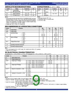
6

 IDT [ INTEGRATED DEVICE TECHNOLOGY ]