IDT72T7285/72T7295/72T72105/72T72115 2.5V TeraSync
16,384 x 72, 32,768 x 72, 65,536 x 72, 131,072 x 72
72-BIT FIFO
COMMERCIAL AND INDUSTRIAL
TEMPERATURE RANGES
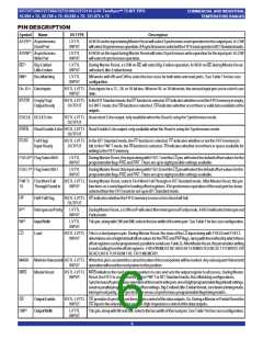
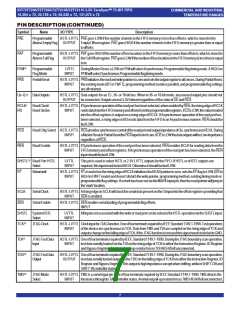
PINDESCRIPTION(CONTINUED)
Symbol
Name
I/OTYPE
Description
PAE
Programmable
HSTL-LVTTL PAEgoes LOWifthe numberofwords inthe FIFOmemoryis less thanoffsetn, whichis storedinthe
Almost-EmptyFlag OUTPUT EmptyOffsetregister. PAEgoes HIGHifthenumberofwords intheFIFOmemoryis greaterthanorequal
tooffsetn.
PAF
Programmable
Almost-FullFlag
HSTL-LVTTL PAFgoesHIGHifthenumberoffreelocationsintheFIFOmemoryismorethanoffsetm,whichisstoredin
OUTPUT theFullOffsetregister.PAFgoesLOWifthenumberoffreelocationsintheFIFOmemoryislessthanorequal
tom.
(1)
PFM
Programmable
Flag Mode
LVTTL DuringMasterReset,aLOWonPFMwillselectAsynchronousProgrammableflagtimingmode.AHIGHon
INPUT
PFMwillselectSynchronousProgrammableflagtimingmode.
PRS
PartialReset
HSTL-LVTTL PRSinitializesthereadandwritepointerstozeroandsetstheoutputregistertoallzeroes.DuringPartialReset,
INPUT
theexistingmode(IDTorFWFT),programmingmethod(serialorparallel),andprogrammableflagsettings
are allretained.
Q0–Q71 DataOutputs
RCLK/ ReadClock/
HSTL-LVTTL Data outputs for an 72-, 36- or 18-bit bus. When in 36- or 18-bit mode, any unused output pins should not
OUTPUT beconnected.Outputsarenot3.3VtolerantregardlessofthestateofOEandRCS.
HSTL-LVTTL IfSynchronousoperationofthereadporthasbeenselected,whenenabledbyREN,therisingedgeofRCLK
RD
ReadStrobe
INPUT
readsdatafromtheFIFOmemoryandoffsetsfromtheprogrammableregisters.IfLDisLOW,thevaluesloaded
intotheoffsetregisters is outputonarisingedgeofRCLK.IfAsynchronous operationofthereadporthas
beenselected,arisingedgeonRDreads datafromtheFIFOinanAsynchronous manner.RENshouldbe
tiedLOW.
RCS
REN
ReadChipSelect HSTL-LVTTL RCSprovidessynchronouscontrolofthereadportandoutputimpedanceofQn,synchronoustoRCLK.During
INPUT
aMasterResetorPartialResettheRCSinputisdon’tcare,ifOEisLOWthedataoutputswillbeLow-Impedance
regardless ofRCS.
ReadEnable
HSTL-LVTTL IfSynchronousoperationofthereadporthasbeenselected,RENenablesRCLKforreadingdatafromthe
INPUT
FIFOmemoryandoffsetregisters.IfAsynchronous operationofthereadporthas beenselected,theREN
inputshouldbetiedLOW.
(1)
RHSTL Read Port HSTL
Select
LVTTL
INPUT
This pin is used to select HSTL or 2.5V LVTTL outputs for the FIFO. If HSTL or eHSTL outputs are
required,thisinputmustbetiedHIGH.OtherwiseitshouldbetiedLOW.
RT
Retransmit
HSTL-LVTTL RTassertedontherisingedgeofRCLKinitializestheREADpointertozero,setstheEFflagtoLOW(ORto
INPUT
HIGHinFWFTmode)anddoesn’tdisturbthewritepointer,programmingmethod,existingtimingmodeor
programmableflagsettings.IfamarkhasbeensetviatheMARKinputpin,thenthereadpointerwilljumpto
the‘mark’location.
SCLK
SerialClock
SerialEnable
HSTL-LVTTL ArisingedgeonSCLKwillclocktheserialdatapresentontheSIinputintotheoffsetregistersprovidingthat
INPUT SEN is enabled.
SEN
HSTL-LVTTL SENenablesserialloadingofprogrammableflagoffsets.
INPUT
SHSTL SystemHSTL
LVTTL
INPUT
AllinputsnotassociatedwiththewriteorreadportcanbeselectedforHSTLoperationviatheSHSTLinput.
Select
(2)
TCK
JTAGClock
HSTL-LVTTL ClockinputforJTAGfunction.OneoffourterminalsrequiredbyIEEEStandard1149.1-1990.Testoperations
INPUT
ofthedevicearesynchronous toTCK.DatafromTMSandTDIaresampledontherisingedgeofTCKand
outputschangeonthefallingedgeofTCK.IftheJTAGfunctionisnotusedthissignalneedstobetiedtoGND.
(2)
TDI
JTAGTestData
Input
HSTL-LVTTL OneoffourterminalsrequiredbyIEEEStandard1149.1-1990.DuringtheJTAGboundaryscanoperation,
INPUT
testdataseriallyloadedviatheTDIontherisingedgeofTCKtoeithertheInstructionRegister,IDRegister
andBypassRegister.Aninternalpull-upresistorforcesTDIHIGHifleftunconnected.
(2)
TDO
JTAGTestData
Output
HSTL-LVTTL OneoffourterminalsrequiredbyIEEEStandard1149.1-1990.DuringtheJTAGboundaryscanoperation,
OUTPUT testdataseriallyloadedoutputviatheTDOonthefallingedgeofTCKfromeithertheInstructionRegister,ID
RegisterandBypassRegister.Thisoutputishighimpedanceexceptwhenshifting,whileinSHIFT-DRand
SHIFT-IRcontrollerstates.
TMS(2)
JTAGMode
Select
HSTL-LVTTL TMS is a serial input pin. One of four terminals required by IEEE Standard 1149.1-1990. TMS directs the
INPUT
thedevicethroughitsTAPcontrollerstates.Aninternalpull-upresistorforcesTMSHIGHifleftunconnected.
7

 IDT [ INTEGRATED DEVICE TECHNOLOGY ]