IDT72T7285/72T7295/72T72105/72T72115 2.5V TeraSync
16,384 x 72, 32,768 x 72, 65,536 x 72, 131,072 x 72
72-BIT FIFO
COMMERCIAL AND INDUSTRIAL
TEMPERATURE RANGES
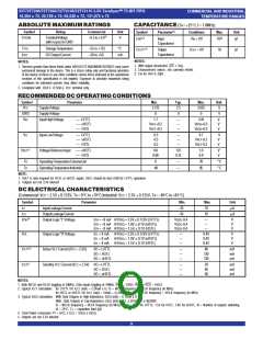
ABSOLUTEMAXIMUMRATINGS
CAPACITANCE(TA = +25°C, f = 1.0MHz)
Symbol
Parameter(1)
Conditions
Max.
Unit
Symbol
Rating
Commercial
Unit
VTERM
TerminalVoltage
with respect to GND
–0.5to+3.6(2)
V
(2,3)
CIN
Input
Capacitance
VIN = 0V
10(3)
pF
(1,2)
TSTG
IOUT
StorageTemperature
DCOutputCurrent
–55 to +125
–50 to +50
°C
mA
COUT
Output
Capacitance
VOUT = 0V
10
pF
NOTES:
NOTES:
1. With output deselected, (OE ≥ VIH).
2. Characterized values, not currently tested.
3. CIN for Vref is 20pF.
1. Stresses greater than those listed under ABSOLUTE MAXIMUM RATINGS may cause
permanent damage to the device. This is a stress rating only and functional operation
of the device at these or any other conditions above those indicated in the operational
sections of this specification is not implied. Exposure to absolute maximum rating
conditions for extended periods may affect reliability.
2. Compliant with JEDEC JESD8-5. VCC terminal only.
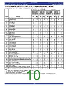
RECOMMENDEDDCOPERATINGCONDITIONS
Symbol
VCC
Parameter
Min.
2.375
0
Typ.
2.5
0
Max.
2.625
0
Unit
V
SupplyVoltage
SupplyVoltage
GND
V
VIH
InputHighVoltage
LVTTL
eHSTL
HSTL
1.7
VREF+0.2
VREF+0.2
—
—
—
3.45
VDDQ+0.3
VDDQ+0.3
V
V
V
VIL
InputLowVoltage
LVTTL
eHSTL
HSTL
-0.3
-0.3
-0.3
—
—
—
0.7
VREF-0.2
VREF-0.2
V
V
V
VREF(1)
VoltageReferenceInput eHSTL
HSTL
0.8
0.68
0.9
0.75
1.0
0.9
V
V
TA
TA
OperatingTemperatureCommercial
OperatingTemperatureIndustrial
0
—
—
70
85
°C
°C
-40
NOTE:
1. VREF is only required for HSTL or eHSTL inputs. VREF should be tied LOW for LVTTL operation.
2. Outputs are not 3.3V tolerant.
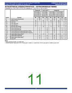
DCELECTRICALCHARACTERISTICS
(Commercial: VCC = 2.5V ± 0.125V, TA = 0°C to +70°C;Industrial: VCC = 2.5V ± 0.125V, TA = -40°C to +85°C)
Symbol
Parameter
Min.
–10
Max.
Unit
ILI
InputLeakageCurrent
OutputLeakageCurrent
OutputLogic“1”Voltage,
10
10
µA
µA
V
V
V
ILO
–10
(5)
VOH
IOH = –8 mA @VDDQ = 2.5V ± 0.125V (LVTTL)
IOH = –8 mA @VDDQ = 1.8V ± 0.1V (eHSTL)
IOH = –8 mA @VDDQ = 1.5V ± 0.1V (HSTL)
VDDQ-0.4
VDDQ-0.4
VDDQ-0.4
—
—
—
VOL
OutputLogic“0”Voltage,
IOL = 8 mA @VDDQ = 2.5V ± 0.125V (LVTTL)
IOL = 8 mA @VDDQ = 1.8V ± 0.1V (eHSTL)
IOL = 8 mA @VDDQ = 1.5V ± 0.1V (HSTL)
—
—
—
0.4V
0.4V
0.4V
V
V
V
ICC1(1,2)
ICC2(1)
Active VCC Current (VCC = 2.5V)
I/O = LVTTL
I/O = HSTL
I/O = eHSTL
—
—
—
80
130
130
mA
mA
mA
Standby VCC Current (VCC = 2.5V) I/O = LVTTL
—
—
—
20
90
90
mA
mA
mA
I/O = HSTL
I/O = eHSTL
NOTES:
1. Both WCLK and RCLK toggling at 20MHz. Data inputs toggling at 10MHz. WCS = HIGH, REN or RCS = HIGH.
2. Typical ICC1 calculation: for LVTTL I/O ICC1 (mA) = 2.24mA x fs, fs = WCLK frequency = RCLK frequency (in MHz)
for HSTL or eHSTL I/O ICC1 (mA) = 55mA + (2.24mA x fs), fs = WCLK frequency = RCLK frequency (in MHz)
3. Typical IDDQ calculation: With Data Outputs in High-Impedance: IDDQ (mA) = 0.15mA x fs
With Data Outputs in Low-Impedance: IDDQ (mA) = (CL x VDDQ x fs x N)/2000
fs = WCLK frequency = RCLK frequency (in MHz), VDDQ = 2.5V for LVTTL; 1.5V for HSTL; 1.8V for eHSTL, N = Number of outputs switching.
tA = 25°C, CL = capacitive load (pf).
4. Total Power consumed: PT = (VCC x ICC) + VDDQ x IDDQ).
5. Outputs are not 3.3V tolerant.
9

 IDT [ INTEGRATED DEVICE TECHNOLOGY ]