IDT72T7285/72T7295/72T72105/72T72115 2.5V TeraSync
16,384 x 72, 32,768 x 72, 65,536 x 72, 131,072 x 72
72-BIT FIFO
COMMERCIAL AND INDUSTRIAL
TEMPERATURE RANGES
1st Parallel Offset Write/Read Cycle
D/Q71
D/Q19
D/Q0
D/Q17
D/Q8
EMPTY OFFSET REGISTER (PAE)
Non-Interspersed
Parity
16
13 12 11 10
9
8
8
7
7
6
6
5
5
1
1
17
17 16 15
15 14
14
4
4
3
3
2
2
Interspersed
Parity
13 12 11 10
9
# of Bits Used
2nd Parallel Offset Write/Read Cycle
D/Q71
D/Q19
D/Q0
D/Q17
D/Q8
FULL OFFSET REGISTER (PAF)
Non-Interspersed
Parity
17 16
13 12 11 10
8
8
7
7
6
6
5
5
15 14
14
9
1
1
4
4
3
3
2
2
Interspersed
Parity
17
15
13 12 11 10 9
16
# of Bits Used
x72 Bus Width
1st Parallel Offset Write/Read Cycle
D/Q35
D/Q35
D/Q19
D/Q19
D/Q0
D/Q17
D/Q8
EMPTY OFFSET REGISTER (PAE)
Non-Interspersed
Parity
16
17
17 16 15
13 12 11 10
9
8
8
7
7
6
6
5
5
1
1
15 14
4
4
3
3
2
2
Interspersed
Parity
14
13 1211 10 9
# of Bits Used
2nd Parallel Offset Write/Read Cycle
D/Q0
D/Q17
D/Q8
FULL OFFSET REGISTER (PAF)
Non-Interspersed
Parity
17 16
13 12 11 10
8
8
7
7
6
6
5
5
15 14
14
9
1
1
4
4
3
3
2
2
Interspersed
Parity
15
13 12 11 10 9
17 16
# of Bits Used
x36 Bus Width
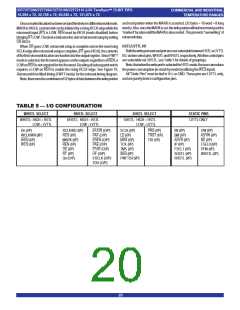
1st Parallel Offset Write/Read Cycle
D/Q17
Data Inputs/Outputs
D/Q16
D/Q0
EMPTY OFFSET (LSB) REGISTER (PAE)
Non-Interspersed
Parity
16 15 14 13 12 11 10
13 12 10
9
8
8
7
7
6
6
5
5
4
4
3
3
2
2
1
1
16
Interspersed
Parity
15 14
11
9
D/Q8
# of Bits Used
2nd Parallel Offset Write/Read Cycle
D/Q17
D/Q16
Data Inputs/Outputs
D/Q0
EMPTY OFFSET (MSB) REGISTER (PAE)
17
17
3rd Parallel Offset Write/Read Cycle
D/Q17
Data Inputs/Outputs
D/Q0
D/Q16
FULL OFFSET (LSB) REGISTER (PAF)
13
10
9
9
8
7
6
5
4
3
3
2
1
1
16 15 14
16 15
12 11
14 13 12 11 10
8
7
6
5
4
2
D/Q8
4th Parallel Offset Write/Read Cycle
# of Bits Used:
D/Q17
D/Q16
Data Inputs/Outputs
14 bits for the IDT72T7285
15 bits for the IDT72T7295
16 bits for the IDT72T72105
17 bits for the IDT72T72115
Note: All unused input bits
are don’t care.
D/Q0
FULL OFFSET (MSB) REGISTER (PAF)
17
17
x18 Bus Width
5994 drw07
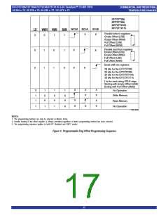
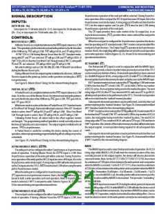
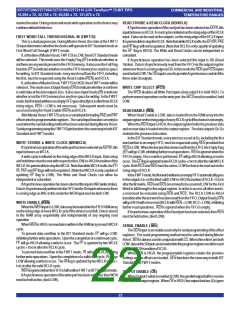
NOTE:
1. Consecutive reads of the offset registers is not permitted. The read operation must be disabled for a minimum of one RCLK cycle in between offset register accesses. (Please
refer to Figure 22, Parallel Read of Programmable Flag Registers (IDT Standard and FWFT Modes) for more details).
Figure 3. Programmable Flag Offset Programming Sequence (Continued)
18

 IDT [ INTEGRATED DEVICE TECHNOLOGY ]