IDT72T7285/72T7295/72T72105/72T72115 2.5V TeraSync
16,384 x 72, 32,768 x 72, 65,536 x 72, 131,072 x 72
72-BIT FIFO
COMMERCIAL AND INDUSTRIAL
TEMPERATURE RANGES
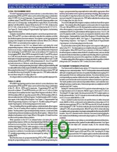
PROGRAMMING FLAG OFFSETS
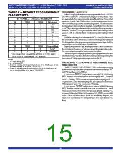
TABLE 2 — DEFAULT PROGRAMMABLE
FLAG OFFSETS
FullandEmptyFlagoffsetvaluesareuserprogrammable.TheIDT72T7285/
72T7295/72T72105/72T72115haveinternalregistersfortheseoffsets.There
areeightdefaultoffsetvalues selectableduringMasterReset.Theseoffset
valuesareshowninTable2.Offsetvaluescanalsobeprogrammedintothe
FIFOinoneoftwoways;serialorparallelloadingmethod.Theselectionofthe
loadingmethodisdoneusingtheLD(Load)pin.DuringMasterReset,thestate
oftheLDinputdetermineswhetherserialorparallelflagoffsetprogrammingis
enabled. A HIGH on LD during Master Reset selects serial loading of offset
values. A LOW on LD during Master Reset selects parallel loading of offset
values.
InadditiontoloadingoffsetvaluesintotheFIFO,itisalsopossibletoread
thecurrentoffsetvalues.Offsetvaluescanbereadviatheparalleloutputport
Q0-Qn,regardlessoftheprogrammingmodeselected(serialorparallel).Itis
notpossibletoreadtheoffsetvaluesinserialfashion.
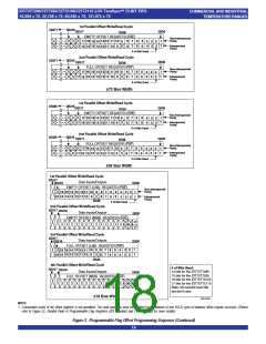
Figure3,ProgrammableFlagOffsetProgrammingSequence,summaries
thecontrolpinsandsequenceforbothserialandparallelprogrammingmodes.
Foramoredetaileddescription,seediscussionthatfollows.
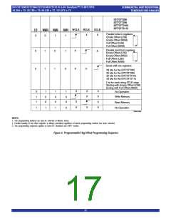
IDT72T7285,72T7295,72T72105,72T72115
*LD
H
L
L
L
FSEL1
FSEL0
Offsets n,m
L
H
L
L
L
H
L
H
L
H
H
1,023
511
255
127
63
31
15
7
L
L
H
H
L
H
H
H
H
*LD
FSEL1
FSEL0
Program Mode
(3)
H
L
X
X
X
X
Serial
Parallel
(4)
The offsetregisters maybe programmed(andreprogrammed)anytime
afterMasterReset,regardlessofwhetherserialorparallelprogramminghas
beenselected. Validprogrammingranges are from0toD-1.
*THIS PIN MUST BE HIGH AFTER MASTER RESET TO WRITE
OR READ DATA TO/FROM THE FIFO MEMORY.
NOTES:
1. n = empty offset for PAE.
SYNCHRONOUS vs ASYNCHRONOUS PROGRAMMABLE FLAG
TIMING SELECTION
TheIDT72T7285/72T7295/72T72105/72T72115canbeconfiguredduring
theMasterResetcyclewitheithersynchronousorasynchronoustimingforPAF
and PAE flags by use of the PFM pin.
2. m = full offset for PAF.
3. As well as selecting serial programming mode, one of the default values will also
be loaded depending on the state of FSEL0 & FSEL1.
4. As well as selecting parallel programming mode, one of the default values will
also be loaded depending on the state of FSEL0 & FSEL1.
If synchronous PAF/PAE configuration is selected (PFM, HIGH during
MRS),thePAFisassertedandupdatedontherisingedgeofWCLKonlyand
notRCLK.Similarly,PAEisassertedandupdatedontherisingedgeofRCLK
onlyandnotWCLK.Fordetailtimingdiagrams,seeFigure23forsynchronous
PAF timingandFigure24forsynchronous PAEtiming.
If asynchronous PAF/PAE configuration is selected (PFM, LOW during
MRS),thePAFisassertedLOWontheLOW-to-HIGHtransitionofWCLKand
PAFisresettoHIGHontheLOW-to-HIGHtransitionofRCLK. Similarly,PAE
isassertedLOWontheLOW-to-HIGHtransitionofRCLK.PAEisresettoHIGH
on the LOW-to-HIGH transition of WCLK. For detail timing diagrams, see
Figure25forasynchronousPAFtimingandFigure26forasynchronousPAE
timing.
15

 IDT [ INTEGRATED DEVICE TECHNOLOGY ]