IC80C51
IC80C31
1. User software should not write 1s to reserved bits. These
bits may be used in future products to invoke new features.
The detail description of each bit is as follows:
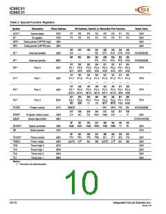
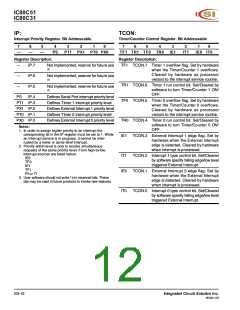
PSW:
Program Status Word. Bit Addressable.
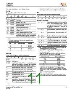
IE:
Interrupt Enable Register. Bit Addressable.
7
6
5
4
3
2
1
0
7
6
5
4
3
2
1
0
CY
AC
F0
RS1 RS0
OV
—
P
EA
—
—
ES
ET1 EX1 ET0 EX0
Register Description:
Register Description:
CY
AC
F0
PSW.7
PSW.6
PSW.5
Carry flag.
Auxiliary carry flag.
EA
IE.7
Disableallinterrupts. IfEA=0, nointerrupt
will be acknowledged. If EA=1, each
interrupt source is individually enabled
or disabled by setting or clearing its
enable bit.
Flag 0 available to the user for
general purpose.
Register bank selector bit 1.(1)
Register bank selector bit 0.(1)
Overflow flag.
RS1 PSW.4
RS0 PSW.3
—
IE.6
IE.5
IE.4
Not implemented, reserve for future use.
(5)
OV
—
P
PSW.2
PSW.1
PSW.0
Usable as a general purpose flag
—
Not implemented, reserve for future use.
(5)
Parity flag. Set/Clear by hardware each
instruction cycle to indicate an odd/even
number of “1” bits in the accumulator.
ES
Enable or disable the serial port interrupt.
ET1 IE.3
Enable or disable the Timer 1 overflow
interrupt.
Note:
1. The value presented by RS0 and RS1 selects the corre-
sponding register bank.
EX1 IE.2
ET0 IE.1
Enable or disable External Interrupt 1.
Enable or disable the Timer 0 overflow
interrupt.
RS1
RS0
Register Bank
Address
00H-07H
08H-0FH
10H-17H
18H-1FH
0
0
1
1
0
1
0
1
0
1
2
3
EX0 IE.0
Enable or disable External Interrupt 0.
Note: To use any of the interrupts in the 80C51 Family, the
following three steps must be taken:
1. Set the EA (enable all) bit in the IE register to 1.
2. Set the coresponding individual interrupt enable bit in
the IE register to 1.
3. Begin the interrupt service routine at the corresponding
Vector Address of that interrupt (see below).
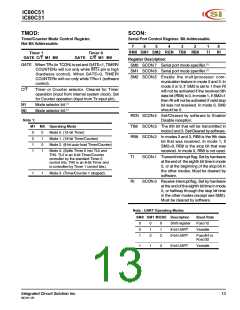
PCON:
Power Control Register. Not Bit Addressable.
Interrupt Source
Vector Address
0003H
7
6
5
4
3
2
1
0
IE0
TF0
SMOD
—
—
—
GF1 GF0
PD IDL
000BH
IE1
0013H
Register Description:
TF1
RI & TI
001BH
0023H
SMOD
Double baud rate bit. If Timer 1 is used to generate
baud rate and SMOD=1, the baud rate is doubled
when the serial port is used in modes 1, 2, or 3.
Not implemented, reserve for future use.(1)
Not implemented, reserve for future use.(1)
Not implemented, reserve for future use.(1)
General purpose flag bit.
4. In addition, for external interrupts, pins INT0 and INT1
(P3.2 and P3.3) must be set to 1, and depending on
whether the interrupt is to be level or transition activated,
bits IT0 or IT1 in the TCON register may need to be set to
0 or 1.
ITX = 0 level activated (X = 0, 1)
ITX = 1 transition activated
5. User software should not write 1s to reserved bits. These
bits may be used in future products to invoke new features.
—
—
—
GF1
GF0
PD
General purpose flag bit.
Power-down bit. Setting this bit activates power-
down mode.
IDL
Idle mode bit. Setting this bit activates idle mode.
operation in the IC80C51/31. If 1s are written to
PD and IDL at the same time, PD takes precedence.
Note:
Integrated Circuit Solution Inc.
MC001-0B
11

 ICSI [ INTEGRATED CIRCUIT SOLUTION INC ]