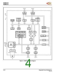
IC80C51
IC80C31
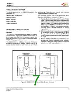
SPECIAL FUNCTION REGISTERS
Accumulator (ACC)
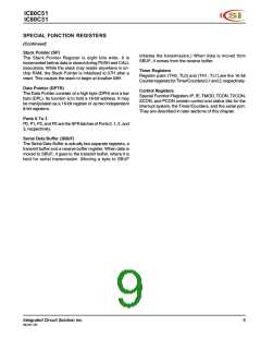
The Special Function Registers (SFR's) are located in
upper 128 Bytes direct addressing area. The SFR Memory
Map in Figure 6 shows that.
ACC is the Accumulator register. The mnemonics for
Accumulator-specific instructions, however, refer to the
Accumulator simply as A.
Not all of the addresses are occupied. Unoccupied
addresses are not implemented on the chip. Read accesses
to these addresses in general return random data, and
write accesses have no effect.
B Register (B)
The B register is used during multiply and divide operations.
For other instructions it can be treated as another scratch
pad register.
User software should not write 1s to these unimplemented
locations, since they may be used in future microcontrollers
to invoke new features. In that case, the reset or inactive
values of the new bits will always be 0, and their active
values will be 1.
Program Status Word (PSW). The PSW register contains
program status information.
The functions of the SFRs are outlined in the following
sections, and detailed in Table 2.
FFH
FF
F8
B
F7
EF
E7
DF
D7
CF
C7
BF
B7
AF
A7
9F
97
F0
E8
E0
D8
D0
C8
C0
B8
B0
A8
A0
98
90
88
80
ACC
PSW
Not Available
in
IC80C51/31
Accessible
by Direct
Addressing
Upper
128
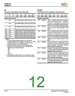
IP
P3
IE
P2
SCON
P1
80H
7FH
80H
SBUF
Accessible
by Direct
and Indirect
Addressing
TCON
P0
8F
87
TMOD
SP
TL0
DPL
TL1
DPH
TH0
TH1
Ports,
Lower
128
PCON
Status and
Control Bits,
Timer,
Special
Function
Registers
Registers,
Stack Pointer,
Accumulator
(Etc.)
Bit
Addressable
0
Figure 6. Internal Data Memory and SFR Memory Map
8 BYTES
78
70
68
60
58
50
48
40
38
30
28
20
18
10
08
00
7F
77
6F
67
5F
57
4F
47
3F
37
2F
27
1F
17
0F
07
SCRATCH
PAD
AREA
BIT
...7F
ADDRESSABLE
SEGMENT
0 ...
BANK3
BANK2
BANK 1
BANK 0
REGISTER
BANKS
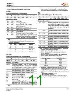
Figure 7. Lower 128 Bytes of Internal RAM
S3-8
Integrated Circuit Solution Inc.
MC001-0B

 ICSI [ INTEGRATED CIRCUIT SOLUTION INC ]