IC80C51
IC80C31
OPERATING DESCRIPTION
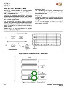
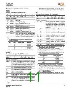
The detail description of the IC80C51 included in this addressing. Figure 6 shows internal data memory
description are:
organization and SFR Memory Map.
• Memory Map and Registers
• Timer/Counters
The lower 128 bytes of RAM can be divided into three
segments as listed below and shown in Figure 7.
1. Register Banks 0-3: locations 00H through 1FH (32
bytes). The device after reset defaults to register bank
0. To use the other register banks, the user must select
them in software. Each register bank contains eight
1-byte registers R0-R7. Reset initializes the stack
point to location 07H, and is incremented once to start
from 08H, which is the first register of the second
register bank.
• Serial Interface
• Interrupt System
• Other Information
MEMORY MAP AND REGISTERS
Memory
2. Bit Addressable Area: 16 bytes have been assigned
for this segment 20H-2FH. Each one of the 128 bits of
this segment can be directly addressed (0-7FH). Each
of the 16 bytes in this segment can also be addressed
as a byte.
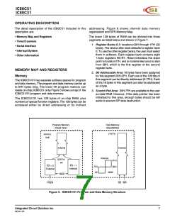
The IC80C51/31 has separate address spaces for program
and data memory. The program and data memory can be up
to 64K bytes long. The lower 4K program memory can
reside on-chip.(IC80C51 only) Figure 5 shows a map of the
IC80C51/31 program and data memory.
3. Scratch Pad Area: 30H-7FH are available to the user
as data RAM. However, if the data pointer has been
initialized to this area, enough bytes should be left
aside to prevent SP data destruction.
The IC80C51/31 has 128 bytes of on-chip RAM, plus
numbers of special function registers. The 128 bytes can be
accessed either by direct addressing or by indirect
Program Memory
(Read Only)
Data Memory
(Read/Write)
FFFFH
FFFFH:
64K
External
External
Internal
FFH
0FFFH:
4K
EA = 1
EA = 0
7FH
00
80H
0000
Internal
External
0000
PSEN
RD WR
Figure 5. IC80C51/31 Program and Data Memory Structure
Integrated Circuit Solution Inc.
MC001-0B
7

 ICSI [ INTEGRATED CIRCUIT SOLUTION INC ]