ICS86953I-147
Integrated
Circuit
Systems, Inc.
LOW
SKEW, 1-TO-9
D
IFFERENTIAL
-
TO-LVCMOS / LVTTL ZERO
DELAY
BUFFER
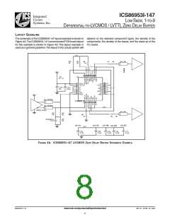
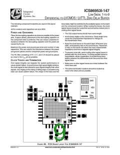
The following component footprints are used in this layout
example:
trace delay might be restricted by the available space on the board
and the component location.While routing the traces, the clock
signal traces should be routed first and should be locked prior to
routing other signal traces.
All the resistors and capacitors are size 0603.
P
OWER AND
G
ROUNDING
• The 50Ω output traces should have same length.
Place the decoupling capacitors as close as possible to the power
pins. If space allows, placement of the decoupling capacitor on
the component side is preferred.This can reduce unwanted in-
ductance between the decoupling capacitor and the power pin
caused by the via.
• Avoid sharp angles on the clock trace.Sharp angle turns
cause the characteristic impedance to change on
the transmission lines.
• Keep the clock traces on the same layer.Whenever pos-
sible, avoid placing vias on the clock traces. Placement
of vias on the traces can affect the trace characteristic
impedance and hence degrade signal integrity.
Maximize the power and ground pad sizes and number of vias
capacitors.This can reduce the inductance between the power
and ground planes and the component power and ground pins.
• To prevent cross talk, avoid routing other signal traces in
parallel with the clock traces. If running parallel traces is
unavoidable, allow a separation of at least three trace
widths between the differential clock trace and the other
signal trace.
The RC filter consisting of R7, C11, and C16 should be placed
as close to the VDDA pin as possible.
C
LOCK
T
RACES AND
TERMINATION
Poor signal integrity can degrade the system performance or
cause system failure. In synchronous high-speed digital systems,
the clock signal is less tolerant to poor signal integrity than other
signals. Any ringing on the rising or falling edge or excessive ring
back can cause system failure. The shape of the trace and the
• Make sure no other signal traces are routed between the
clock trace pair.
• The series termination resistors should be located as
close to the driver pins as possible.
GND
50 Ohm
Trace
VDD
R1
C1
R7
VCCA
C16
VIA
Other
signals
U1
Pin 1
C11
C5
C4
R2
C2
C3
50 Ohm
Trace
FIGURE 4B. PCB BOARD LAYOUT FOR ICS86953I-147
86953BYI-147
www.icst.com/products/hiperclocks.html
REV. B APRIL 23, 2004
9

 ICSI [ INTEGRATED CIRCUIT SOLUTION INC ]