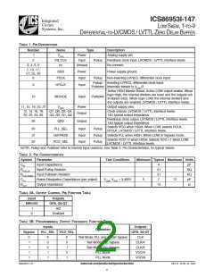
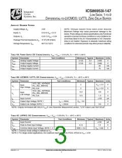
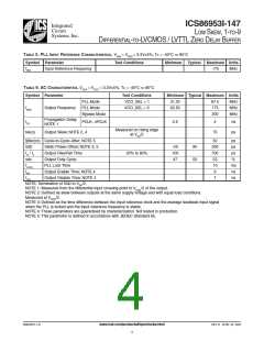
ICS86953I-147
Integrated
Circuit
Systems, Inc.
LOW
SKEW, 1-TO-9
D
IFFERENTIAL
-
TO-LVCMOS / LVTTL ZERO
DELAY
BUFFER
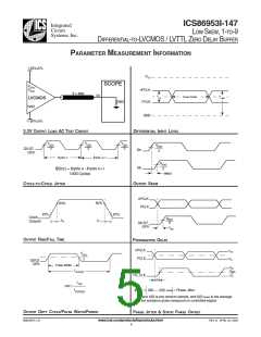
APPLICATION INFORMATION
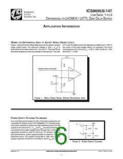
WIRING THE DIFFERENTIAL INPUT TO ACCEPT SINGLE ENDED LEVELS
Figure 1 shows how the differential input can be wired to accept of R1 and R2 might need to be adjusted to position theV_REF in
single ended levels. The reference voltage V_REF = VDD/2 is the center of the input voltage swing. For example, if the input
generated by the bias resistors R1, R2 and C1.This bias circuit clock swing is only 2.5V andVDD = 3.3V, V_REF should be 1.25V
should be located as close as possible to the input pin.The ratio and R2/R1 = 0.609.
VDD
R1
1K
Single Ended Clock Input
PCLK
V_REF
nPCLK
C1
0.1u
R2
1K
FIGURE 1. SINGLE ENDED SIGNAL DRIVING DIFFERENTIAL INPUT
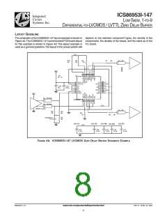
POWER SUPPLY FILTERING TECHNIQUES
As in any high speed analog circuitry, the power supply pins are
vulnerable to random noise.The ICS86953I-147 provides sepa-
rate power supplies to isolate any high switching noise from the
outputs to the internal PLL.VDDA and VDDO should be individually
connected to the power supply plane through vias, and bypass
capacitors should be used for each pin. To achieve optimum
jitter performance, power supply isolation is required. Figure 2
illustrates how a 10Ω resistor along with a 10µF and a .01µF
bypass capacitor should be connected to each VDDA pin.
3.3V
VDDO
.01µF
.01µF
10Ω
VDDA
10 µF
FIGURE 2. POWER SUPPLY FILTERING
86953BYI-147
www.icst.com/products/hiperclocks.html
REV. B APRIL 23, 2004
6

 ICSI [ INTEGRATED CIRCUIT SOLUTION INC ]