ICS86953I-147
Integrated
Circuit
Systems, Inc.
LOW
SKEW, 1-TO-9
D
IFFERENTIAL
-
TO-LVCMOS / LVTTL ZERO
DELAY
BUFFER
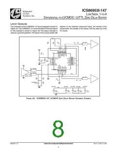
LAYOUT GUIDELINE
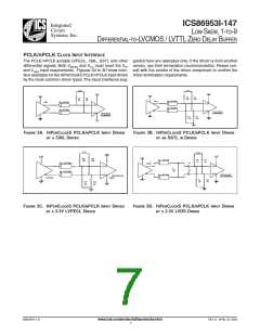
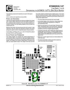
The schematic of the ICS86953I-147 layout example is shown in depend on the selected component types, the density of the
Figure 4A.The ICS86953I-147 recommended PCB board layout components, the density of the traces, and the stack up of the
for this example is shown in Figure 4B. This layout example is P.C.board.
used as a general guideline.The layout in the actual system will
VDD
R10
1K
R8
1K
R9
1K
R1
36
Zo = 50
VDD
U1
R7
10 - 15
24
23
22
21
20
19
18
17
1
VDDA
Q1
VDDO
Q2
GND
Q3
VDDO
Q4
GND
2
3
4
5
6
7
8
FB_CLK
nc
nc
nc
nc
GND
PCLK
C16
10u
C11
0.01u
VCC
Zo = 50 Ohm
Zo = 50 Ohm
ICS86953I-147
VDD
LVPECL Driv er
Zo = 50
R3
50
R4
50
R6
1K
R2
36
C6 (Option)
0.1u
R5
50
(U1-15)
(U1-11)
(U1-19) (U1-23)
(U1-27)
VDD
C2
0.1uF
C3
0.1uF
C4
0.1uF
C5
0.1uF
C1
0.1uF
F
IGURE 4A. ICS86953I-147 LVCMOS ZERO
D
ELAY
B
UFFER
SCHEMATIC
E
XAMPLE
86953BYI-147
www.icst.com/products/hiperclocks.html
REV. B APRIL 23, 2004
8

 ICSI [ INTEGRATED CIRCUIT SOLUTION INC ]