ICS86953I-147
Integrated
Circuit
Systems, Inc.
LOW
SKEW, 1-TO-9
D
IFFERENTIAL
-
TO-LVCMOS / LVTTL ZERO
DELAY
BUFFER
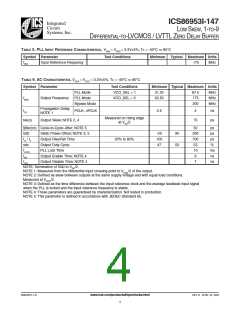
TABLE 5. PLL INPUT REFERENCE CHARACTERISTICS, VDDA = VDDO = 3.3V 5ꢀ, TA = -40°C TO 85°C
Symbol Parameter Test Conditions Minimum Typical Maximum Units
fREF Input Reference Frequency 175 MHz
TABLE 6. AC CHARACTERISTICS, VDDA = VDDO = 3.3V 5ꢀ, TA = -40°C TO 85°C
Symbol Parameter
Test Conditions
VCO_SEL = 1
VCO_SEL = 0
Minimum Typical Maximum Units
PLL Mode
31.25
62.50
87.5
175
200
MHz
MHz
MHz
fMAX
Output Frequency
PLL Mode
Bypass Mode
Propagation Delay;
NOTE 1
tPD
PCLK, nPCLK
2.5
4
ns
ps
Measured on rising edge
at VDD/2
tsk(o)
Output Skew; NOTE 2, 4
75
tjitter(cc) Cycle-to-Cycle Jitter; NOTE 5
50
200
700
53
10
6
ps
ps
ps
ꢀ
t(Ø)
tR / tF
odc
tLOCK
tEN
Static Phase Offset; NOTE 3, 5
Output Rise/Fall Time
-20
100
47
90
50
20ꢀ to 80ꢀ
Output Duty Cycle
PLL Lock Time
ms
ns
ns
Output Enable Time; NOTE 4
Output Disable Time; NOTE 4
tDIS
7
NOTE: Termination of 50Ω to VDD/2.
NOTE 1: Measured from the differential input crossing point to VDDO/2 of the output.
NOTE 2: Defined as skew between outputs at the same supply voltage and with equal load conditions.
Measured at VDDO/2.
NOTE 3: Defined as the time difference between the input reference clock and the average feedback input signal
when the PLL is locked and the input reference frequency is stable.
NOTE 4: These parameters are guaranteed by characterization. Not tested in production.
NOTE 5: This parameter is defined in accordance with JEDEC Standard 65.
86953BYI-147
www.icst.com/products/hiperclocks.html
REV. B APRIL 23, 2004
4

 ICSI [ INTEGRATED CIRCUIT SOLUTION INC ]