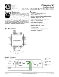
ICS86953I-147
Integrated
Circuit
Systems, Inc.
LOW
SKEW, 1-TO-9
D
IFFERENTIAL
-
TO-LVCMOS / LVTTL ZERO
DELAY
BUFFER
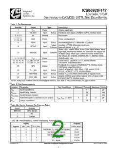
TABLE 1. PIN DESCRIPTIONS
Number
Name
VDDA
Type
Description
1
2
Power
Input
Analog supply pin.
FB_CLK
nc
Pullup
Feedback clock input. LVCMOS / LVTTL interface levels.
No connect.
3, 4, 5, 6
Unused
7, 13, 17,
21, 25, 29
GND
PCLK
nPCLK
Power
Input
Input
Power supply ground.
8
Pullup
Non-inverting LVPECL differential clock input.
Pullup/ Inverting LVPECL differential clock input.
Pulldown Internally biased to VDDO/2.
9
Active HIGH Master Reset. Active LOW output enable. When
logic High, the internal dividers are reset and the outputs are
tri-stated (HiZ). When logic LOW, the internal dividers and
the outputs are enabled. LVCMOS / LVTTL interface levels.
10
MR/nOE
VDDO
Input
Pulldown
11, 15, 19, 23, 27
Power
Output
Output supply pins.
12, 14, 16, 18,
20, 22, 24, 26
Q7, Q6, Q5, Q4,
Q3, Q2, Q1, Q0
Clock outputs. LVCMOS / LVTTL interface levels.
14Ω typical output impedance.
Feedback clock output. LVCMOS / LVTTL interface levels.
14Ω typical output impedance.
28
QFB
Output
Selects VCO when HIGH. When LOW, selects PCLK,
nPCLK. LVCMOS / LVTTL interface levels.
30
31
32
PLL_SEL
nBYPASS
VCO_SEL
Input
Input
Input
Pullup
Pullup
Pullup
Selects PLL when HIGH. When LOW, in Bypass mode.
Selects VCO ÷2 when HIGH. Selects VCO ÷1 when LOW.
LVCMOS / LVTTL interface levels.
NOTE: Pullup and Pulldown refer to internal input resistors. See Table 2, Pin Characteristics, for typical values.
TABLE 2. PIN CHARACTERISTICS
Symbol
CIN
Parameter
Test Conditions
Minimum Typical Maximum Units
Input Capacitance
Input Pullup Resistor
4
pF
KΩ
KΩ
pF
Ω
RPULLUP
51
51
7
RPULLDOWN Input Pulldown Resistor
CPD
Power Dissipation Capacitance (per output)
Output Impedance
VDDA, VDDO = 3.465V
5
12
ROUT
14
TABLE 3A. OUTPUT CONTROL PIN FUNCTION TABLE
Input
Outputs
QFB, Q0:Q7
HiZ
MR/nOE
1
0
Enabled
TABLE 3B. PROGRAMMABLE OUTPUT FREQUENCY FUNCTION TABLE
Inputs
Outputs
QFB, Q0:Q7
CLK
Operation
Bypass
PLL_SEL VCO_SEL
0
1
1
1
1
X
0
0
1
1
X
0
1
0
1
Test Mode: PLL and divider bypass
Test Mode: PLL bypass
Test Mode: PLL bypass
PLL Mode
CLK/4
CLK/8
VCO/4
PLL Mode
VCO/8
86953BYI-147
www.icst.com/products/hiperclocks.html
REV. B APRIL 23, 2004
2

 ICSI [ INTEGRATED CIRCUIT SOLUTION INC ]