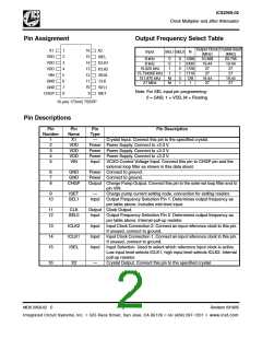
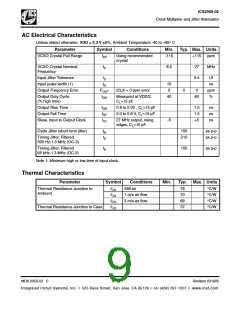
ICS2059-02
Clock Multiplier and Jitter Attenuator
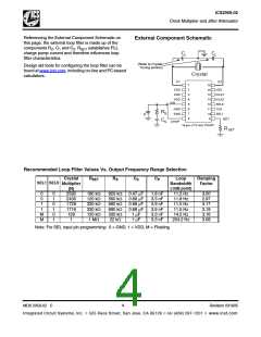
In most cases the load capacitors will not be required.
They should not be stuffed on the prototype evaluation
board as the indiscriminate use of these trim capacitors
will typically cause more crystal centering error than
their absence. If the need for the load capacitors is later
determined, the values will fall within the 1-4 pf range.
The need for, and value of, these trim capacitors can
only be determined at prototype evaluation. Please
refer to MAN05 for the procedure to determine the
component values.
The ICS Applications Note MAN05 may also be
referenced for additional suggestions on layout of the
crystal section.
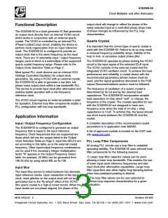
PCB Layout Recommendations
For optimum device performance and lowest output
phase noise, the following guidelines should be
observed. Please also refer to the Recommended PCB
Layout drawing on page 7.
1) Each 0.01µF decoupling capacitor should be
mounted on the component side of the board as close
to the VDD pin as possible. No vias should be used
between decoupling capacitor and VDD pin. The PCB
trace to VDD pin should be kept as short as possible,
as should the PCB trace to the ground via. Distance of
the ferrite bead and bulk decoupling from the device is
less critical.
2) The loop filter components must also be placed
close to the CHGP and VIN pins. C should be closest
P
to the device. Coupling of noise from other system
signal traces should be minimized by keeping traces
short and away from active signal traces. Use of vias
should be avoided.
3) The external crystal should be mounted just next to
the device with short traces. The X1 and X2 traces
should not be routed next to each other with minimum
spaces, instead they should be separated and away
from other traces.
4) To minimize EMI, the 33Ω series termination resistor
(if needed) should be placed close to the clock output.
5) An optimum layout is one with all components on the
same side of the board, minimizing vias through other
signal layers (the ferrite bead and bulk decoupling
capacitor can be mounted on the back). Other signal
traces should be routed away from the ICS2059-02.
This includes signal traces just underneath the device,
or on layers adjacent to the ground plane layer used by
the device.
MDS 2059-02 C
6
Revision 031605
Integrated Circuit Systems, Inc. ● 525 Race Street, San Jose, CA 95126 ● tel (408) 297-1201 ● www.icst.com

 ICSI [ INTEGRATED CIRCUIT SOLUTION INC ]