ICS2059-02
Clock Multiplier and Jitter Attenuator
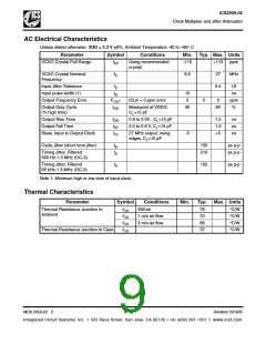
AC Electrical Characteristics
Unless stated otherwise, VDD = 3.3 V 5%, Ambient Temperature -40 to +85° C
Parameter
Symbol
Conditions
Min. Typ. Max. Units
VCXO Crystal Pull Range
f
Using recommended
crystal
-115
+115
ppm
XP
VCXO Crystal Nominal
Frequency
f
X
8.5
27
MHz
Input Jitter Tolerance
Input pulse width (1)
Output Frequency Error
t
0.4
UI
ns
ji
t
10
0
pi
F
ICLK = 0 ppm error
Measured at VDD/2,
0
0
ppm
%
OUT
Output Duty Cycle
(% high time)
t
40
60
OD
C =15 pF
L
Output Rise Time
t
0.8 to 2.0V , C =15 pF
1.5
1.5
+5
ns
ns
ns
OR
L
Output Fall Time
t
2.0 to 0.8 V, C =15 pF
OF
L
Skew, Input to Output Clock
t
27 MHz output, rising
-5
IO
edges, C =15 pF
L
Cycle Jitter (short term jitter)
t
150
210
ps p-p
ps p-p
ja
Timing Jitter, Filtered
t
jf
500 Hz-1.3 MHz (OC-3)
Timing Jitter, Filtered
t
150
ps p-p
jf
65 kHz-1.3 MHz (OC-3)
Note 1: Minimum high or low time of input clock.
Thermal Characteristics
Parameter
Symbol
Conditions
Min.
Typ. Max. Units
Thermal Resistance Junction to
Ambient
θ
θ
θ
Still air
78
70
68
37
°C/W
°C/W
°C/W
°C/W
JA
JA
JA
JC
1 m/s air flow
3 m/s air flow
Thermal Resistance Junction to Case
θ
MDS 2059-02 C
9
Revision 031605
Integrated Circuit Systems, Inc. ● 525 Race Street, San Jose, CA 95126 ● tel (408) 297-1201 ● www.icst.com

 ICSI [ INTEGRATED CIRCUIT SOLUTION INC ]