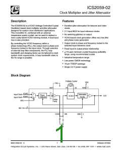
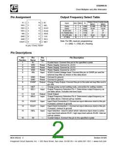
ICS2059-02
Clock Multiplier and Jitter Attenuator
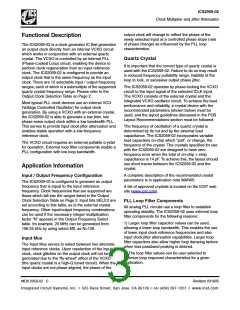
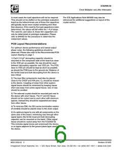
Referencing the External Component Schematic on
this page, the external loop filter is made up of the
External Component Schematic
CL CL
components R , C and C . R establishes PLL
Z
1
2
SET
charge pump current and therefore influences loop
filter characteristics.
(Refer to Crystal
Tuning section)
Design aid tools for configuring the loop filter can be
found at www.icst.com, including on-line and PC-based
calculators.
Crystal
X1
X2
1
2
3
4
5
6
7
8
16
15
14
13
12
11
VDD
VDD
VDD
ISEL
ICLK1
ICLK2
SEL0
CLK
VIN
GND
GND
RS
CS
SEL1
10
9
P
ISET
CHGP
16-pin (173 mil) TSSOP
RSET
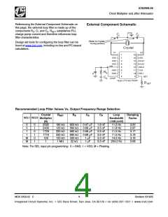
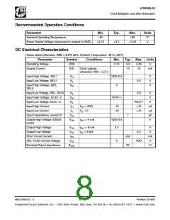
Recommended Loop Filter Values Vs. Output Frequency Range Selection
Crystal
Multiplier
(N)
R
R
C
C
P
Loop
Bandwidth
(-3dB point)
Damping
Factor
SET
S
S
SEL1 SEL0
0
0
1
1
M
M
0
1
0
1
0
1
2592
2430
1728
1716
128
180 kΩ
120 kΩ
330 kΩ
330 kΩ
120 kΩ
1 MΩ
820 kΩ
560 kΩ
680 kΩ
680 kΩ
330 kΩ
22 kΩ
0.47 µF
0.68 µF
0.68 µF
0.68 µF
1 µF
1.8 nF
3.3 nF
3.9 nF
3.9 nF
3.3 nF
3.3 nF
11.2 Hz
11.8 Hz
11.5 Hz
11.5 Hz
14.5 Hz
204.2 Hz
3.00
2.97
3.17
3.18
3.16
3.08
1
1 µF
Note: For SEL input pin programming: 0 = GND, 1 = VDD, M = Floating
MDS 2059-02 C
4
Revision 031605
Integrated Circuit Systems, Inc. ● 525 Race Street, San Jose, CA 95126 ● tel (408) 297-1201 ● www.icst.com

 ICSI [ INTEGRATED CIRCUIT SOLUTION INC ]