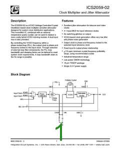
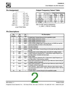
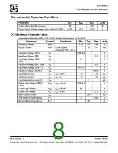
ICS2059-02
Clock Multiplier and Jitter Attenuator
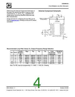
A “normalized” PLL loop bandwidth may be calculated
as follows:
Series Termination Resistor
Clock output traces over one inch should use series
termination. To series terminate a 50Ω trace (a
commonly used trace impedance), place a 33Ω resistor
in series with the clock line, as close to the clock output
pin as possible. The nominal impedance of the clock
output is 20Ω. (The optional series termination resistor
is not shown in the External Component Schematic.)
RS × ICP ×354755
NBW = ---------------------------------------
N
The “normalized” bandwidth equation above does not
take into account the effects of damping factor or the
second pole. However, it does provide a useful
approximation of filter performance.
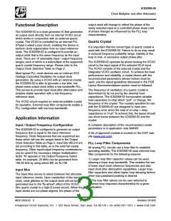
Decoupling Capacitors
As with any high-performance mixed-signal IC, the
ICS2059-02 must be isolated from system power
supply noise to perform optimally.
The loop damping factor is calculated as follows:
375
625 × I
× C
CP
S
Damping Factor = R ×
-----------------------------------------
Decoupling capacitors of 0.01µF must be connected
between each VDD and the PCB ground plane. To
further guard against interfering system supply noise,
the ICS2059-02 should use one common connection to
the PCB power plane as shown in the diagram on the
next page. The ferrite bead and bulk capacitor help
reduce lower frequency noise in the supply that can
lead to output clock phase modulation.
S
N
Where:
R = Value of resistor in loop filter (Ohms)
S
I
= Charge pump current (amps)
CP
(refer to Charge Pump Current Table, below)
N = Crystal multiplier shown in the above table
C = Value of capacitor C in loop filter (Farads)
S
1
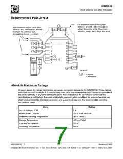
Recommended Power Supply Connection
for Optimal Device Performance
As a general rule, the following relationship should be
maintained between components C and C in the loop
VDD Pin
Ferrite
1
2
filter:
Bead
Connection to 3.3V
VDD Pin
Power Plane
C
S
C = -----
P
20
Bulk Decoupling Capacitor
(such as 1 F Tantalum)
VDD Pin
Charge Pump Current Table
0.01 F Decoupling Capacitors
Charge Pump Current
(ICP
RSET
)
1.4 MΩ
680 kΩ
540 kΩ
120 kΩ
10 µA
20 µA
25 µA
100 µA
Crystal Load Capacitors
The device crystal connections should include pads for
small capacitors from X1 to ground and from X2 to
ground, shown as C in the External Component
L
Schematic. These capacitors are used to adjust the
stray capacitance of the board to match the nominally
required crystal load capacitance. Because load
capacitance can only be increased in this trimming
process, it is important to keep stray capacitance to a
minimum by using very short PCB traces (and no vias)
been the crystal and device.
Special considerations must be made in choosing loop
components C and C These recommendations can
be found in the design aid tools section of
www.icst.com.
S
P.
MDS 2059-02 C
5
Revision 031605
Integrated Circuit Systems, Inc. ● 525 Race Street, San Jose, CA 95126 ● tel (408) 297-1201 ● www.icst.com

 ICSI [ INTEGRATED CIRCUIT SOLUTION INC ]