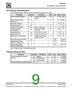
ICS2059-02
Clock Multiplier and Jitter Attenuator
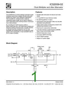
Pin Assignment
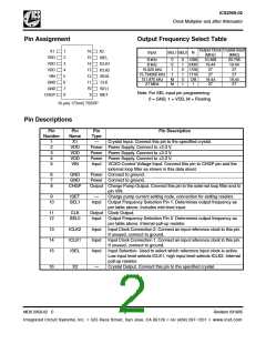
Output Frequency Select Table
Output Clock CrystalUsed
X1
VDD
VDD
VDD
VIN
1
2
3
4
5
6
7
8
16
15
14
13
12
11
10
9
X2
Input
SEL1 SEL0
N
(MHz)
10.368
19.44
27
(MHz)
20.736
19.44
27
ISEL
ICLK1
ICLK2
SEL0
CLK
8 kHz
8 kHz
15.625 kHz
15.734265 kHz
151.875 kHz
27 MHz
0
0
0
1
0
1
0
1
1296
2430
1728
1716
128
1
1
27
27
M
M
19.44
27
19.44
27
GND
GND
CHGP
1
SEL1
ISET
Note: For SEL input pin programming:
0 = GND, 1 = VDD, M = Floating
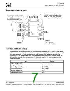
16- pin( 173mil) TSSOP
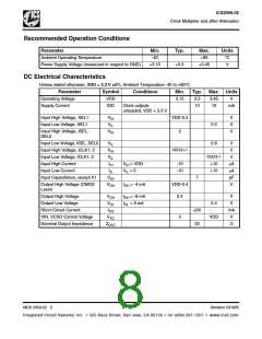
Pin Descriptions
Pin
Pin
Pin
Pin Description
Number
Name
Type
1
2
3
4
5
X1
—
Crystal Input. Connect this pin to the specified crystal.
VDD
VDD
VDD
VIN
Power Power Supply. Connect to +3.3 V.
Power Power Supply. Connect to +3.3 V.
Power Power Supply. Connect to +3.3 V.
Input
VCXO Control Voltage Input. Connect this pin to CHGP pin and the
external loop filter as shown in this data sheet.
6
7
8
GND
GND
CHGP
Power Connect to ground.
Power Connect to ground.
Output Charge Pump Output. Connect this pin to the external loop filter and to
pin VIN.
9
10
ISET
SEL1
—
Input
Charge pump current setting node, connection for setting resistor.
Output Frequency Selection Pin 1. Determines output frequency as
per table above. Includes mid-level input.
11
12
CLK
SEL0
Output Clock Output.
Input
Input
Input
Input
Output Frequency Selection Pin 0. Determines output frequency as
per table above. Internal pull-up resistor.
Input Clock Connection 2. Connect an input reference clock to this pin.
If unused, connect to ground.
Input Clock Connection 1. Connect an input reference clock to this pin.
If unused, connect to ground.
Input Selection. Used to select which reference input clock is active.
Low input level selects ICLK1, high input level selects ICLK2. Internal
pull-up resistor.
13
14
15
ICLK2
ICLK1
ISEL
16
X2
—
Crystal Output. Connect this pin to the specified crystal.
MDS 2059-02 C
2
Revision 031605
Integrated Circuit Systems, Inc. ● 525 Race Street, San Jose, CA 95126 ● tel (408) 297-1201 ● www.icst.com

 ICSI [ INTEGRATED CIRCUIT SOLUTION INC ]