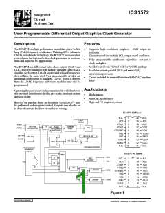
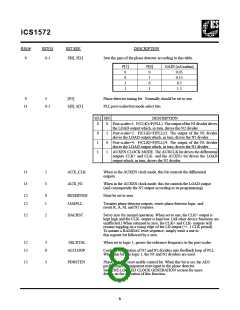
ICS1572
This allows the synthesizer to be completely programmed for An additional control pin on the ICS1572-301, BLANK can
the desired frequency before it is made active. Once the part perform either of two functions. It may be used to disable the
has been “unlocked” by the 32 writes, programming becomes phase-frequency detector in line-locked applications. Alterna-
effective immediately.
tively, the BLANK pin may be used as a synchronous enable
forVRAMshift clockgeneration.Seesections onLine-Locked
ALL registers identified in the data sheet (0-9, 11, 12 & 15) Operations and VRAM shift clock generation for details.
MUSTbewrittenuponinitial programming.Theprogramming
registers are not initialized upon power-up, but the latched
outputs of those registers are. The latch is made transparent
after 32 register writes. If any register has not been written, the
Output Description
The differential output drivers, CLK+ and CLK, are current-
mode and are designed to drive resistive terminations in a
complementary fashion. The outputs are current-sinking only,
with the amount of sink current programmable via the IPRG
pin. The sink current, whichis steered toeither CLK+orCLK-,
is approximately four times the current supplied to the IPRG
pin. For most applications, a resistor fromVDDO to IPRG will
set the current to the necessary precision. See Figure 6 for
output characteristics.
stateupon power-up (random) willbecome effective. Registers
13 & 14 physically do not exist. Register 10 does exist, but is
reserved for future expansion. To insure compatibility with
possiblefuture modifications to thedatabase, ICS recommends
that all three unused locations be written with zero.
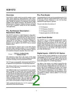
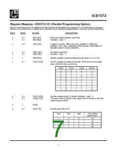
ICS1572-101 Register Loading
5
The LOAD output is a high-current CMOS type drive whose
frequency is controlled by a programmable divider that may be
selected for a modulus of 3, 4, 5, 6, 8, or 10. It may also be
suppressed under register control.
STROBE
1
2
3
4
AD0-AD3
ADDRESS VALID
DATA VALID
The LD/N2 output is high-current CMOS type drive whose
frequency is derived from the LOAD output. The programma-
ble modulus may range from 1 to 512 in steps of one.
Figure 2
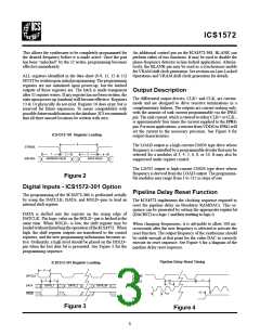
Digital Inputs - ICS1572-301 Option
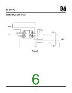
The programming of the ICS1572-301 is performed serially
by using the DATCLK, DATA, and HOLD~pins to load an
internal shift register.
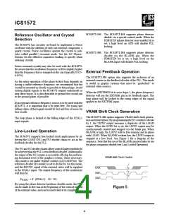
Pipeline Delay Reset Function
The ICS1572 implements the clocking sequence required to
reset the pipeline delay on Brooktree RAMDACs. This se-
quence can be generated by setting the appropriate register bit
(DACRST) to a logic 1 and then resetting to logic 0.
DATA is shifted into the register on the rising edge of
DATCLK. The logic value on the HOLD~ pin is latched at the
same time. When HOLD~ is low, the shift register may be
loadedwithoutdisturbingtheoperation of theICS1572. When
high, the shift register outputs are transferred to the control
registers, and the new programming information becomes ac-
tive. Ordinarily, a high level should be placed on the HOLD~
pin when the last data bit is presented. See Figure 3 for the
programming sequence.
When changing frequencies, it is advisable to allow 500 mi-
croseconds after the new frequency is selected to activate the
reset function. The output frequency of the synthesizer should
be stable enough at that point for the video DAC to correctly
execute its reset sequence. See Figure 4 for a diagram of the
pipeline delay reset sequence.
Pipeline Delay Reset Timing
ICS1572-301 Register Loading
8
DATCLK
STROBE
or
11
6
7
10
9
DATCLK
CLK+
DATA
HOLD
DATA_1
DATA_2
DATA_56
12
TCLK
LOAD
Figure 3
Figure 4
3

 ICSI [ INTEGRATED CIRCUIT SOLUTION INC ]