ICS1572
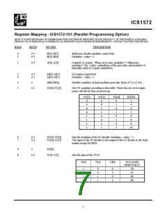
REG#
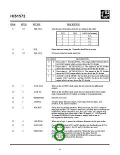
9
BIT(S)
0-1
BIT REF.
P[0]..P[1]
DESCRIPTION
Sets the gain of the phase detector according to this table.
P[1]
P[0]
0
GAIN (uA/radian)
0
0
1
1
0.05
0.15
0.5
1
0
1
1.5
9
3
[P2]
Phase detector tuning bit. Normally should be set to one.
PLL post-scaler/test mode select bits
11
0-1
S[0]..S[1]
S[1] S[0]
DESCRIPTION
0
0
1
1
0
1
0
1
Post-scaler=1. F(CLK)=F(PLL). Theoutput of theN1 divider drives
the LOAD output which, in turn, drives the N2 divider.
Post-scaler=2. F(CLK)=F(PLL)/2. The output of the N1 divider
drives the LOAD output which, in turn, drives the N2 divider.
Post-scaler=4. F(CLK)=F(PLL)/4. The output of the N1 divider
drives the LOAD output which, in turn, drives the N2 divider.
AUXEN CLOCK MODE. The AUXCLK bit drives the differential
outputs CLK+ and CLK- and the AUXN1 bit drives the LOAD
output which, in turn, drives the N2 divider.
11
11
2
3
AUX_CLK
AUX_N1
When in the AUXEN clock mode, this bit controls the differential
outputs.
When in the AUXEN clock mode, this bit controls the LOAD output
(and consequently the N2 output according to its programming).
12
12
0
1
RESERVED
JAMPLL
Must be set to zero.
Tristates phase detector outputs; resets phase detector logic, and
resets R, A, M, and N2 counters.
12
2
DACRST
Set to zero for normal operation. When set to one, the CLK+ output is
kept high and the CLK- output is kept low. (All other device functions are
unaffected.) When returned to zero, the CLK+ and CLK- outputs will
resume toggling on a rising edge of the LD output (+/- 1 CLK period).
To initiate a RAMDAC reset sequence, simply write a one to
this register bit followed by a zero.
12
15
3
0
SELXTAL
ALTLOOP
When set to logic 1, passes the reference frequency to the post-scaler.
Controls substitution of N1 and N2 dividers into feedback loop of PLL.
When this bit is a logic 1, the N1 and N2 dividers are used.
15
3
PDRSTEN
Phase-detector reset enable control bit. When this bit is set, the AD3
pin becomes a transparent reset input to the phase detector.
See LINE-LOCKED CLOCK GENERATION section for more
details on the operation of this function.
8

 ICSI [ INTEGRATED CIRCUIT SOLUTION INC ]