ICS1531 Data Sheet - Preliminary
Chapter 6 Register Set
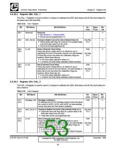
6.5.40.4 Register 3Bh: CAL_1
The CAL_1 Register is used to select (1) delays to calibrate the ADC data delay and (2) the clock delay for
the green and red channels.
Table 6-42. CAL1 Register
Bit
Bit Name
Bit Definition
Ac-
cess
Spec.
Func.
Re-
set
R•esSeerveeSde.ction 6.1, “Reserved Bits”.
• This bit can be programmed to ‘0’.
3B:7
Reserved
–
–
0
A•naTlhoigs-btoit-wDoigrkitsalwCithonRveegrste3rCD:4ataan(dG3lCob:3alf)orDaelgaloyb[a0l].delay
3B:6
ADC_DD [0]
G_CD
See Reg
37:3
–
0
of all RGB data output from the ADC.
• This bit is the least-significant bit.
Green (Channel) Clock Delay.
3B:5-
3B:3
R/W
–
–
5
5
These bits select a delay (that is, an offset) for use in
calibrating the clock for the green channel. (An acknowledge See Reg
of these bits occurs only when the Calibration Regs are
37:3
e•na0b,lethde.) cWlohcekndtehleasyecbailtibsraarteio:n offset is 0.
• 1 or above, the clock delay calibration offset increases.
3B:2
3B:0
R_CD
Red (Channel) Clock Delay.
These bits select a delay (that is, an offset) for use in
R/W
calibrating the clock for the red channel. (An acknowledge of See Reg
these bits occurs only when the Calibration Regs are
37:3
e•na0b,lethde.) cWlohcekndtehleasyecbailtibsraarteio:n offset is 0.
• 1 or above, the clock delay calibration offset increases.
6.5.40.5 Register 3Ch: CAL_2
The CAL_2 Register is used to select (1) delays to calibrate the ADC data delay and (2) the clock delay for
blue channel.
Table 6-43. CAL2 Register
Bit
Bit Name
Bit Definition
Ac-
Spec. Re-
cess
Func.
set
3C:7-
3C:5
Bandgap_CAL Bandgap Calibration.
To calibrate the ICS1531 bandgap voltage, these bits adjust
R/W
–
5
the current to VRTR, VRTG, and VRTB. (An acknowledge
occurs only when the Test mode is enabled.)
A•naTlohegs-teob-DitsigwitoarlkCwointhveRretegr3DBa:6tafo(Gr alogblaolb)aDl delealayy[2o-f1a]l.l
3C:4-
3C:3
ADC_DD [2-1]
B_CD
See Reg
37:3
–
–
0
5
RGB data output from the ADC.
• These bits are the most-significant bits.
Blue (Channel) Clock Delay.
3C:2-
3C:0
R/W
These bits select a delay (that is, an offset) for use in
calibrating the clock for the blue channel. (An acknowledge See Reg
of these bits occurs only when the Calibration Regs are
enabled.) When these bits are:
37:3
• 0, the clock delay calibration offset is 0.
• 1 or above, the clock delay calibration offset increases.
ICS1531 Rev N 12/1/99
December, 1999
Copyright © 1999, Integrated Circuit Systems, Inc.
All rights reserved.
53

 ICSI [ INTEGRATED CIRCUIT SOLUTION INC ]