ICS1531 Data Sheet - Preliminary
Chapter 6 Register Set
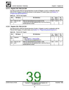
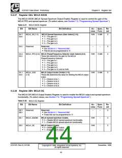
6.5.21 Register 24h: PNLCLK-SSOE
The PNLCLK-SSOE (PNLCLK Spread-Spectrum Output Enable) Register is used to control the gain of the
PNLCLK PFD and spread spectrum. (To select values, see Section 7.3, “Programming Spread Spectrum”.)
Table 6-21. PNLCLK-SSOE Register
Bit
Bit Name
Bit Definition
Ac- Spec.
cess Func.
Re-
set
24:7- PNLCLK_SS
PNLCLK Spread-Spectrum (Gain Select) [1-0].
R/W
D-PK
0
24:6
24:5
[1-0]
T•he0se=bTithsedgeateinrmisin1e. the PNLCLK spread-spectrum gain.
• 1 = The gain is 2.
• 2 = The gain is 4.
• 3 = The gain is 8.
R•esSeerveeSde.ction 6.1, “Reserved Bits”.
• This bit can be programmed to ‘0’.
PNLCLK Phase/Frequency Detector (Gain Select) [2-0].
These bits determine the PNLCLK Phase/Frequency
Reserved
–
–
0
0
24:4- PNLCLK_PFD
24:2 [2-0]
R/W
D-PK
D•et0ec=toTrhgeaigna.in is 1.
• 1 = The gain is 2.
• 2 = The gain is 4.
• 3 = The gain is 8.
• 4 = The gain is 16, and so forth.
24:1- PNLCLK_OSD
24:0 [1-0]
PNLCLK Output Scaler Divider (Value) [1-0].
These bits determine the value for dividing the PNLCLK
output scaler as follows:
R/W
D-PK
0
• 0 = Division is by 1.
• 1 = Division is by 2.
• 2 = Division is by 4.
• 3 = Division is by 8.
ICS1531 Rev N 12/1/99
December, 1999
Copyright © 1999, Integrated Circuit Systems, Inc.
All rights reserved.
40

 ICSI [ INTEGRATED CIRCUIT SOLUTION INC ]