IBM3009K2672
IBM SONET/SDH Framer
155.52 MHz (only for the pseudo-ECL input). Additionally, a divided-down version of the synthesized transmit
SONET/SDH clock is provided on the TXDCLK pin. This pin can be enabled or disabled via the Tx_DivEnt bit
in the SIMTConf2 register. The frequency of the divided clock on the TXDCLK pin can be selected via the
Tx_DivFrq(2:0) control bits in the SIMTConf1 register to be either 19.44, 38.88, 51.84, or 77.76 MHz. In the
receive direction, divided-down versions of the recovered clocks from the four macros are provided on four
pins (RXDCLK#). The frequencies of the clocks on the RXDCLK# pins can be individually selected to be
either 19.44, 38.88, 51.84, or 77.76 MHz via the Rx_DivFrq#(2:0) bits in the SIMRConf1 and SIMRConf2 reg-
isters. The Rx_DivEnt# bits in the SIMRConf4 register can be used to enable or disable the outputs of their
respective RXDCLK# pins.
A byte-parallel interface is provided for STM-16/STS-48 multi-device applications as well as byte-parallel
STM-4/4c/STS-12/12c single device applications. Off-chip byte clock recovery and synthesis are required
when using the byte-parallel interface. The receive parallel data must be byte-aligned to the bytes in the
incoming SONET/SDH frame.
Four low power inputs (TXLPOW#) and Loss of Signal inputs (LOSSSIG#) are provided for monitoring exter-
nal interface circuitry for low power or loss of signal conditions. Also a lock detect status input is provided to
monitor external clock recovery circuitry. When any of these pins are asserted high, a corresponding
maskable interrupt request bit is set. Five control pins (TXSDOWN# and RSTCREC1) are provided for con-
trolling external line interface circuitry via the register map of the SONET/SDH framer. The TXSDOWN# pins
can be used to turn the lasers of a fiber optic module on or off. The RSTCREC1 pin can be used to reset an
external clock recovery device.
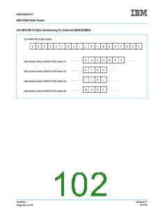
When the byte-parallel line interface is used, a Frame Pulse input (FP1) is provided by an external deserial-
izer/demux to identify the frame boundary. The A2Frm(1:0) bits in the OFPRXGP2 register can be pro-
grammed to indicate the location of the FP1 pulse in the RXPDAT1(7:0) stream. An OOF1 control signal is
provided for controlling the byte and frame synchronization for an external deserializer/demux device. OOF1
is asserted to indicate to the external deserializer/demux device to resynch to the SONET/SDH frame pattern.
If an out of frame condition does not exist, OOF1 is low. If then n (n=4 or 5, configurable) consecutive bad
framing patterns are received, OOF1 goes high. This should cause the external deserializer/demux device to
resynchronize to the framing pattern. The external deserializer/demux will pulse FP1 high for one clock cycle
as it resynchronizes. If the next framing pattern after the pulse on FP1 is correct, the OOF1 will be driven low
and remain low. If this framing pattern is incorrect, OOF1 will be driven low for two clock cycles and then
driven high again to force the deserializer/demux device to resynchronize to the frame pattern. If three con-
secutive frame periods elapse since the low to high transition of OOF1 and no pulse has been received on
FP1, OOF1 will be driven low for two clock cycles and then driven high again.
Operation
ssframer.01
8/27/99
Page 90 of 279

 IBM [ IBM ]