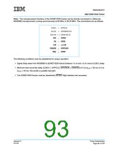
IBM3009K2672
IBM SONET/SDH Framer
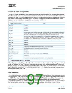
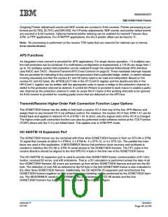
Chiplet-to-Clock Assignments
The GPPCLK input signal needs to be present to operate the GPPINT chiplet. The corresponding clocks for
the other chiplets need to be present or access to those chiplets via the microprocessor interface will not suc-
ceed and will result in the watchdog timer timing out and a corresponding interrupt not being issued. The chip-
lets and the corresponding clocks that need to be present in order to access them are listed below. In the
table and the text that follow, # refers to the macro number: 1, 2, 3, or 4.
:
Chiplet / External Interface
ACI_Tx1
Clock
TXUCLK1
TXUCLK2
RXUCLK1
RXUCLK2
ACI_Tx2
ACI_Rx1
ACI_Rx2
Depends on the setting of the PHT#(2:0) bits in the PHTXGP1 and PHTXGP2 global configuration
registers. The clock can be either TXUCLK1, TXUCLK2, or ACHCLK (internal transit mode). If the
PHT#(2:0) and PHR#(2:0) bits are contradictory, the PHT#(2:0) setting takes priority.
PH_Tx#
PH_Rx#
Depends on the setting of the PHR#(2:0) bits in the PHRXGP1 and PHRXGP2 global configura-
tion registers. The clock can be either RXUCLK1, RXUCLK2, or ACHCLK (internal transit mode).
If the PHT#(2:0) and PHR#(2:0) bits are contradictory, the PHT#(2:0) setting takes priority.
ACH_Tx#
ACHCLK
ACH_Rx#
ACHCLK
PPP
ACHCLK
OFP_Tx#
Transmit line clock synthesized from REFCLKT/E or TX_BYCLKINT/E.
Corresponding recovered receive line clock or RXBYCLK1.
GPPCLK
OFP_Rx#
GPPINT
Transmit Telecom Bus
Receive Telecom Bus
TXTB#CLK
Corresponding recovered receive line clock or RXBYCLK1.
AIP_TX1
TXRINGCLK
1
Transmit line clock synthesized from REFCLKT/E or TX_BYCLKINT/E.
AIP_RX
1. External interfaces, part of OFP_xxx chiplets.
Other chiplets, or parts of chiplets, have their clocks selected according to global configuration parameter set-
tings. For example, the ACB_Tx# FIFOs write logic has the same clock as the corresponding PH_Tx# port
handler, whereas the read logic is always clocked by ACHCLK. The SDB_Tx# FIFO’s write port can be driven
by TXTB#CLK (if GContTx# = ’11’) or ACHCLK (GContTx# /= ’11’), whereas the read logic is always driven
by the same clock as OFP_Tx#.
Line Interfaces
The SONET/SDH framer provides four serial line interfaces with differential I/O and integrated clock recovery
and synthesis for STM-1/4/4c or STS-3c/STS-12/12c applications. Line Interface #1 can handle 622.08 Mb/s
or 155.52 Mb/s data rates. Line interfaces #2 - #4 handle 155.52 Mb/s data rates. Either of two reference
clock sources (TTL or differential pseudo-ECL) for transmit clock synthesis can be selected via the
Tx_RefSelS control bit in the SIMTConf2 register. The frequency of the reference clocks can be selected via
the Tx_RefFrq(2:0) control bits in the SIMTConf1 register to be either 19.44, 38.88, 51.84, 77.76, or
ssframer.01
8/27/99
Operation
Page 89 of 279

 IBM [ IBM ]