IBM3009K2672
IBM SONET/SDH Framer
Operation
This Operation section provides additional detailed information on the operation of the functional units and
processes of the SONET/SDH framer. It is by no means exhaustive and should be read in conjunction with
the information contained in the other sections of this databook.
It should be noted that interrupt requests are not rationalized in the SONET/SDH framer hardware. That is,
lower level alarms are not inhibited by higher level alarms. The rationalization of alarms needs to be handled
in the software that monitors the SONET/SDH framer.
Memory Map Bit Ordering
The memory map of the SONET/SDH framer is partitioned into named “chiplet” segments, as shown in the
table Chiplet Address Map on page 110. Chiplets are synonymous with “functional blocks”. Several chiplets
can make up a higher level functional block, like those shown in the High Level Block Diagram on page 7. For
example, the UTOPIA Level1/2/2+ block in the block diagram is made up of the ACI_xxx and PH_xxx chip-
lets, the APH block is composed of the ACH_xxx and PPP chiplets, the SFH blocks are composed of the
OFP_xxx chiplets, the Telecom Bus block is not composed of chiplets but is controlled by the GPPINT and
OFP_xxx chiplets, the LIU blocks are also not composed of chiplets but are controlled by the GPPINT chiplet,
and the T/RACC is a part of the ACH_xxx chiplets.
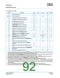
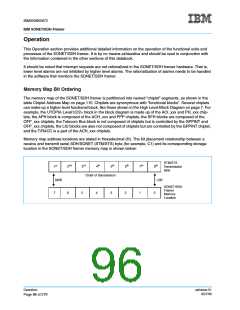
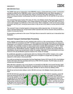
Memory map address locations are stated in Hexadecimal (H). The bit placement relationship between a
receive and transmit serial SDH/SONET (STM/STS) byte (for example, C1) and its corresponding storage
location in the SONET/SDH framer memory map is shown below:
STM/STS
Transmission
Byte
2nd
3rd
4th
5th
6th
7th
8th
1st
Order of transmission
MSB
LSB
SONET/SDH
Framer
Memory
7
6
5
4
3
2
1
0
Location
Operation
ssframer.01
8/27/99
Page 88 of 279

 IBM [ IBM ]